Samsung Unveils Shiny U.S. Headquarters
Get Tom's Hardware's best news and in-depth reviews, straight to your inbox.
You are now subscribed
Your newsletter sign-up was successful
Samsung Electronics held the opening ceremony for its new state-of-the-art $300 million 1.1 million square feet, 10-story building and campus on Thursday in San Jose, California.
Built on the razed site of its previous 214,000 square foot campus, and covering a total of 9.4 acres, the site, which includes approximately 636,000 sq. ft. of office and lab space and can hold up to 2000 employees, is 100 percent owned by Samsung.
Housing the North American headquarters for the Device Solutions (components) businesses for Samsung Electronics, the new facility is also home to several of the firm's research labs, as well as sales and marketing staff for the Device Solutions America headquarters. It currently boasts some 700 employees, with the firm noting that primary hiring for the next decade at the facility will be for R&D.
Article continues belowSamsung's Device Solutions businesses are focused on providing semiconductor, display and other component technologies for consumer electronics, smartphones, tablets, PCs, home appliances and the Internet of Things.
Opened just two years after the initial groundbreaking ceremony, the building dedication was attended by local government officials, Samsung partners, executives and hundreds of staff, all uniformed in Samsung blue.
San Jose's mayor, Sam Liccardo, said approval of the site's permit took just 54 working days, while Mike Rossi, California governor Jerry Brown's senior business advisor, said that by supporting Samsung, the state had made a "good investment" that was already paying dividends.
Dr. O.H Kwon, CEO and Vice Chairman of Samsung electronics, said the facility would help Samsung ramp to a "more aggressive pace of growth" over the next few decades, and that the firm planned to fill it to capacity with "2,000 of Silicon Valley's best and brightest talent."
Get Tom's Hardware's best news and in-depth reviews, straight to your inbox.
"We are determined to drive the leading edge of innovation in the semiconductor industry," he added.
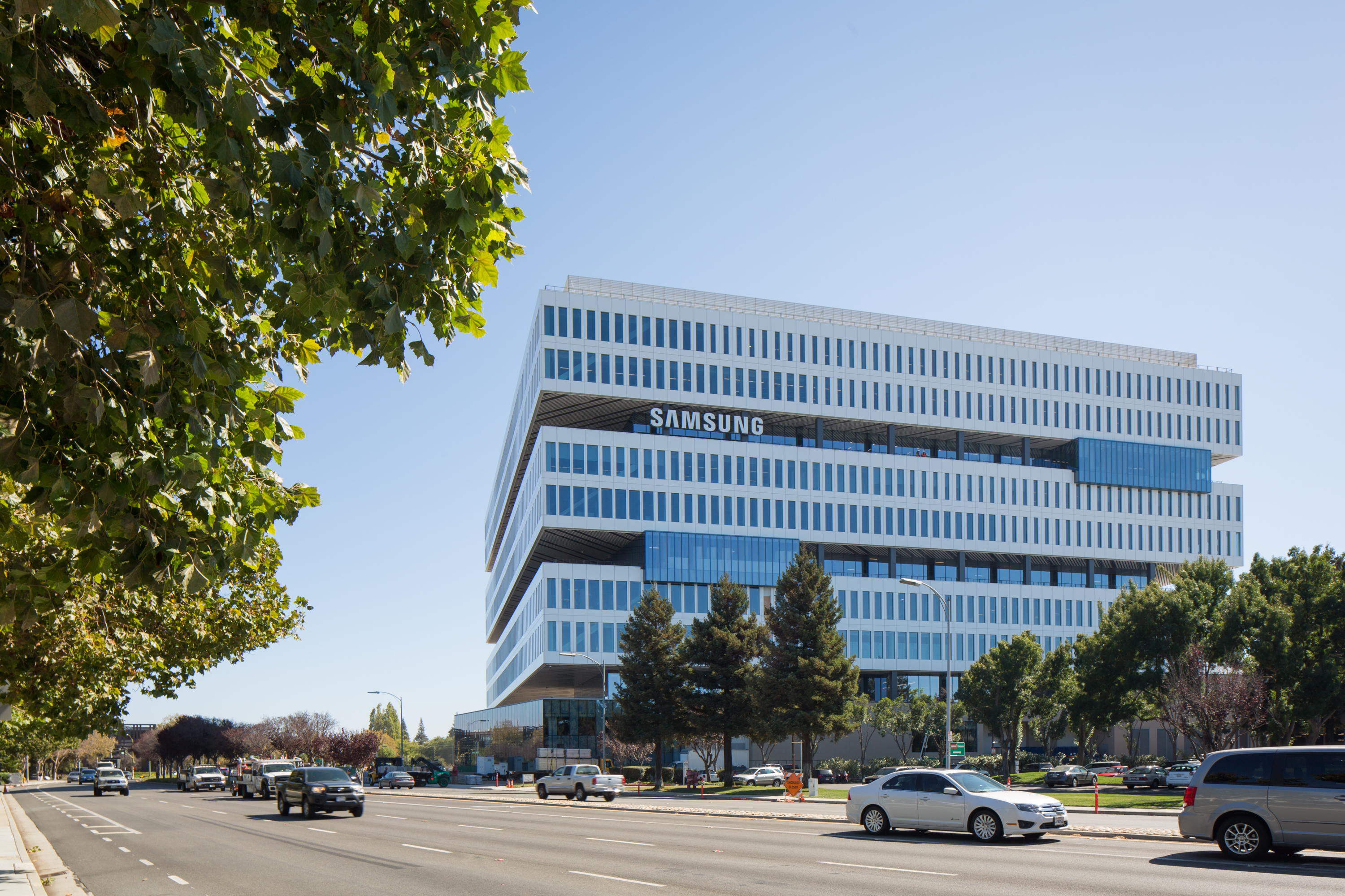
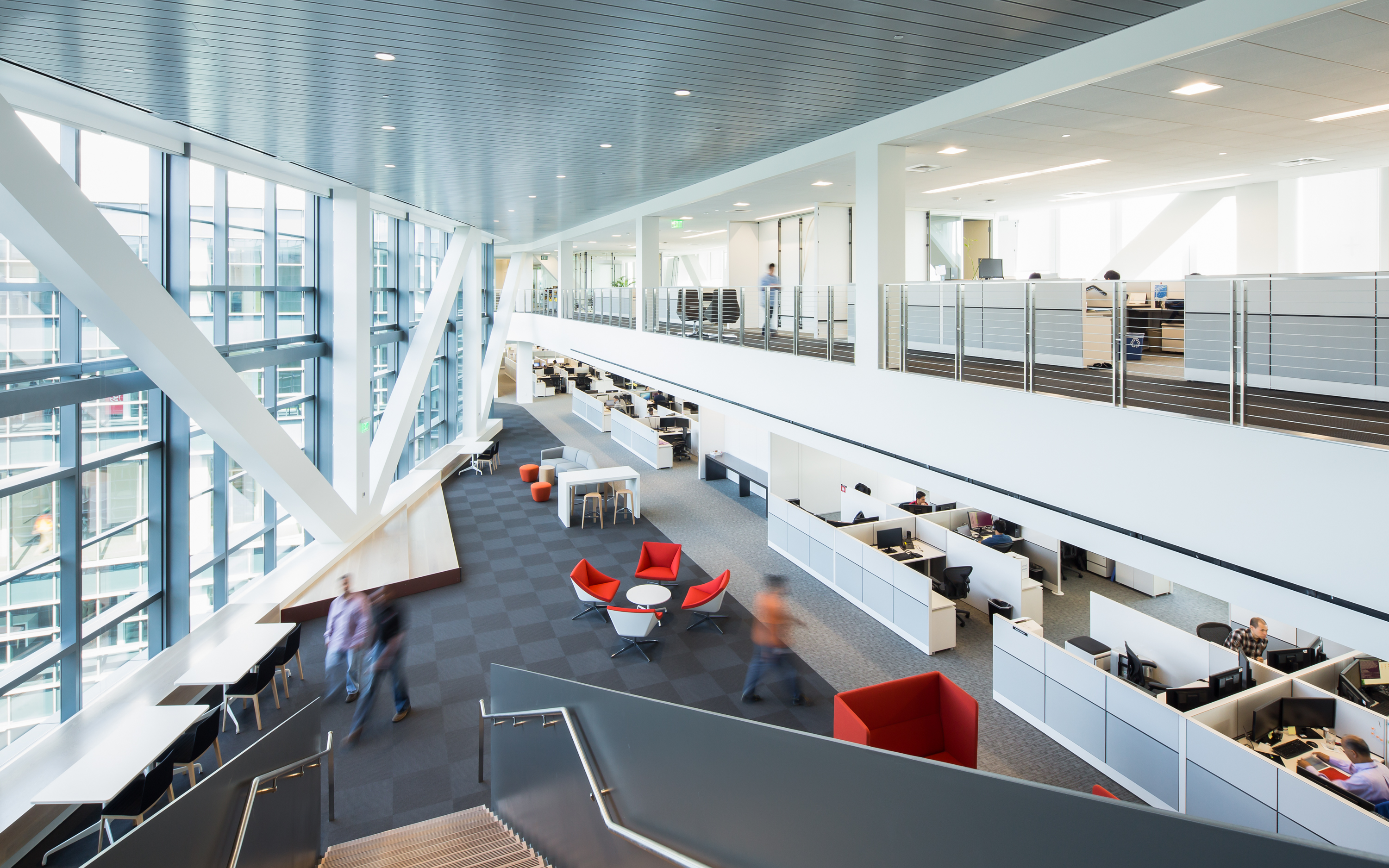
The building itself is certainly innovative, built as a series of two-story office "buildings" stacked on top of one another, sandwiching a series of "green floors" with gardens and recreational opportunities that are part of an effort to re-introduce the natural environment in office architecture.
The architects behind the structure are NBBJ, while the construction was undertaken by Webcor Builders.
The facility is clad in white metal, punctuated by a series of windows that vary in width, making it look like a chip stack from the outside, and an airy, open, glass space from the inside.
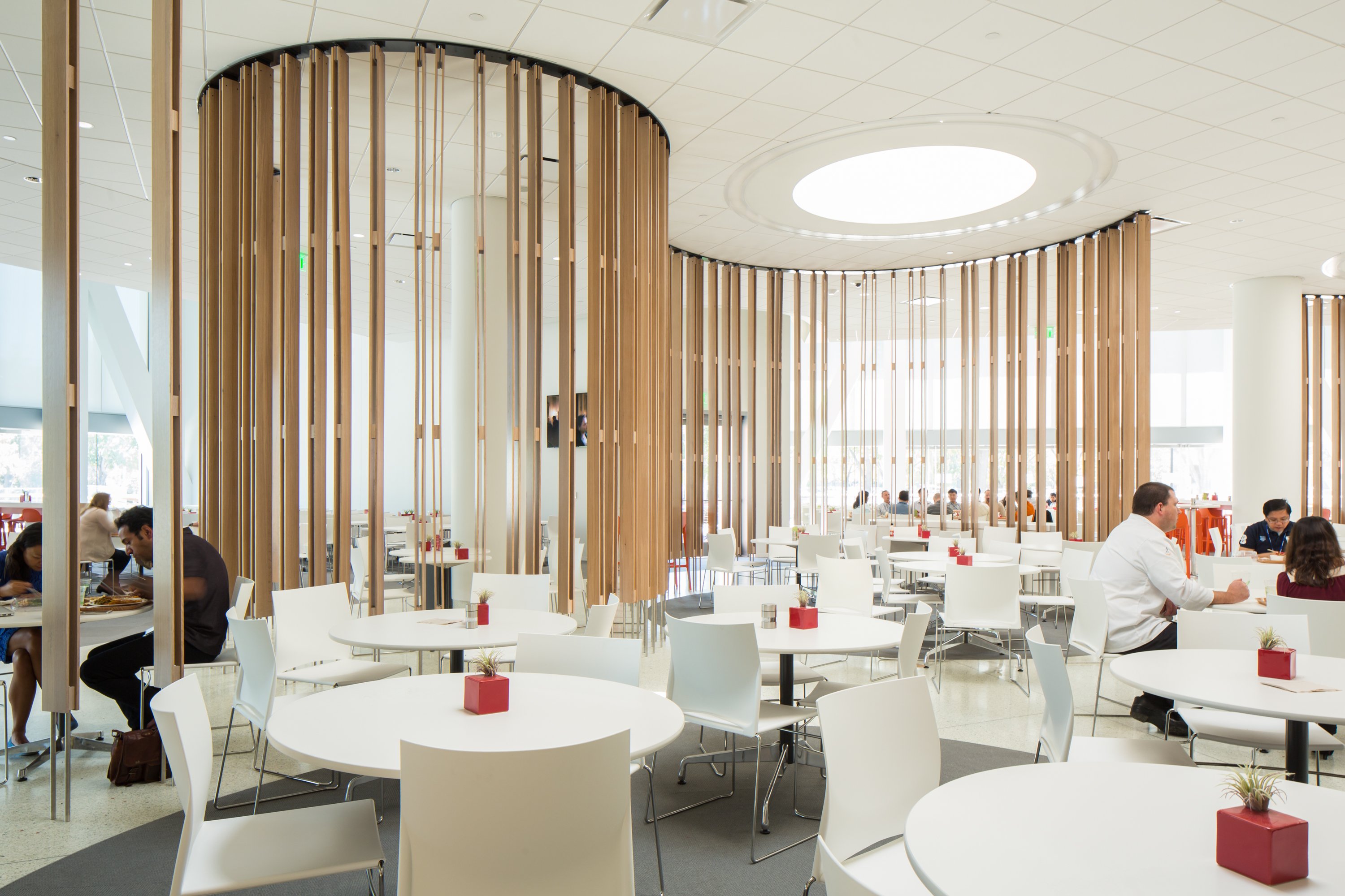
The wider windows are aligned with shared communal spaces for extra natural daylight, and campus amenities include large gardens of varying dimensions and character, an expansive fitness facility, and a large star-shaped cafeteria building capable of seating up to 750 diners. The cafeteria covers 20,158 square feet of space, and it provides one free and subsequently subsidized meals to all employees.
The 170-foot tall building has been designed to the LEED (Leadership in Energy and Environmental Design) standards of the U.S. Green Building Council.
The firm said the new building would not mean that it will close other facilities outside of Northern California. In 2014 alone, Samsung Electronics' total investment in R&D was $13.7 billion, around 6.9 percent of its overall sales for that year.
Most recently, Samsung's R&D has been working on SSD products for the data center and cloud computing, with software to speed up and enhance the drives.
Meanwhile, in the world of displays, Samsung boasted that it has developed the world's fastest display interface systems to drive next-generation ultra-high resolution screens, and a display data compression codec adopted by all of the major chip makers, as well as a methodology for evaluating visual display quality that has been accepted as a part of the JPEG standard.
Wrapping up the ceremony, Samsung executives discussed how the new facility would increase the economic development of San Jose and talked about the firm's corporate responsibility and outreach programs with local non-profits like the Second Harvest Food Bank and the Family Giving Tree.
The firm said its employees volunteered many service hours with both groups, and it presented them each a check for $100,000.
Samsung also said it was putting greater emphasis on STEM, by setting up an education scholarship fund for college age students in STEM programs at California state universities or the University of California. One student per year will receive funding for his or her enrollment and living expenses.
The ceremony concluded with a reminder of the facility's new tagline: Collaborate, innovate, grow.
Follow us @tomshardware, on Facebook and on Google+.
-
kawininjazx I wish our own American companies would be headquartered here and building places like this.Reply -
mlee 2500 ReplyI wish our own American companies would be headquartered here and building places like this.
Uh....have you SEEN the new Apple campus? -
overclockingrocks *impressed whistle* fancy. I like how it's ultra modern and the fact the building looks like a chip stack from outside makes me chuckle in a good way. Way to go Samsung!Reply -
Chris Droste this looks really nice, however I've already been inside of Chrysler's Tech Center in Auburn Hills, MI which is over 4million sq feet. architecturally this is pretty nice but it's nothing unorthodox.Reply -
Mephisto666 @jayracer , keep your Republican BS off this site please.... FYI there will be another Dem in the Presidency once the current Pres is gone. Dry those tears :)Reply


