SK Hynix's 300-Layer 3D NAND to Increase SSD Performance and Lower Costs
300-layer 3D NAND to increase performance and bit density.

SK Hynix recently published details about its 8th-Gen 3D NAND memory device with over 300 active layers. The company's new 3D NAND devices will enable it to increase the performance of SSDs and lower their per-TB costs when it arrives sometime in the 2024 to 2025 timeframe.
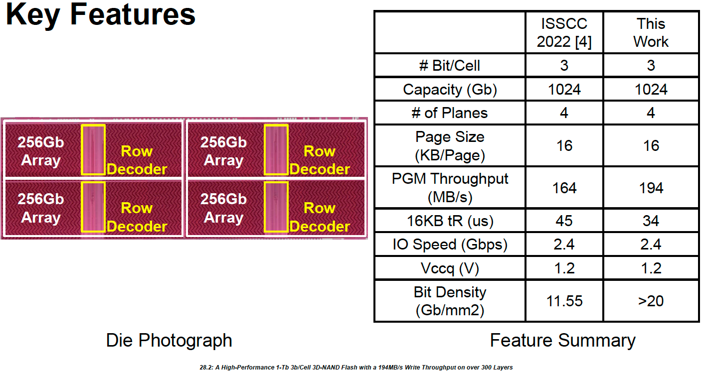
SK Hynix's initial 8th-Gen 3D NAND device with 300+ layers will come with a 1Tb (128GB) capacity with triple level cells and a bit density of over 20Gb/mm^2. In addition, the chip features a 16KB page size, four planes, a 2400 MT/s interface, and a maximum throughput of 194 MB/s (18% higher than 7th-Gen 238-layer 3D NAND). The high-speed I/O and increased throughput will be particularly useful for the best SSDs featuring a PCIe 5.0 x4 or a more advanced interface.

Nearly doubling the bit density of the new NAND will significantly increase the per-wafer productivity of the new manufacturing node, which will lower SK Hynix's costs, though it is unclear how significantly.
To improve the design, SK Hynix had to implement five new schemes:
- Triple-Verify Program (TPGM) feature that narrows cell threshold voltage distribution and reduces tPROG (program time) by 10%, which translates into higher performance;
- Adaptive Unselected String Pre-Charge (AUSP) — another procedure to reduce tPROG by around 2%;
- All-Pass Rising (APR) scheme that reduces tR (read time) by approximately 2% and cuts word line rising time;
- Programmed Dummy String (PDS) technique that cuts world line settling time for tPROG and tR by reducing channel capacitance load;
- Plane-Level Read Retry (PLRR) capability that allows to change read level of a plane without terminating others therefore issuing subsequent read commands immediately and improving quality of service (QoS) and therefore read performance.
SK Hynix didn't disclose when it plans to start producing its 8th Generation 3D NAND devices. However, since the company has disclosed details about this technology, it looks like its development has been completed or is close to completion. Meanwhile, because all flash memory makers tend to slow down the adoption of newer manufacturing nodes to limit NAND bit output, it's unlikely that SK Hynix will rush 8th Gen 3D NAND to production. Therefore, it's rational to expect the new memory to be adopted in 2024.
Get Tom's Hardware's best news and in-depth reviews, straight to your inbox.

Anton Shilov is a contributing writer at Tom’s Hardware. Over the past couple of decades, he has covered everything from CPUs and GPUs to supercomputers and from modern process technologies and latest fab tools to high-tech industry trends.
-
DaveLTX Reply
This isn't a QLC SSD. Speed increases usually comes with TBW increases as well.Amdlova said:Speed incrases tbw decrases :) you can bench two times before tears apart -
bit_user ReplySK Hynix's initial 8th-Gen 3D NAND device with 300+ layers will come with a 1Tb (128GB) capacity with triple level cells
They're not. They're 3-bit cells = 8 levels.
I know the industry-standard nomenclature is TLC, but don't expand it out when doing so just misleads people!