Joengdong Choe, Senior Technical Fellow at TechInsights, Inc., gave two presentations during the 2020 Flash Memory Summit detailing the future of 3D NAND and other emerging memories. TechInsights is known for its analysis and reverse engineering of multiple semiconductor products including flash.
Choe’s presentation this year included a 2014-2023 roadmap along with some discussion of general trends in the flash industry. This discussion covered both TLC and QLC parts from all major manufacturers, including Samsung, Kioxia (formerly Toshiba), Intel, Micron, SK hynix, and YMTC. Choe covered several aspects of these designs, from layer count to CMOS (peripheral circuitry) placement and other architectural factors that can impact bit density and cost.
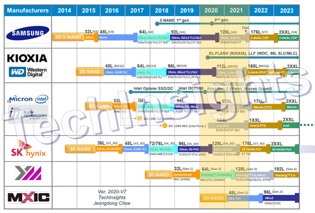
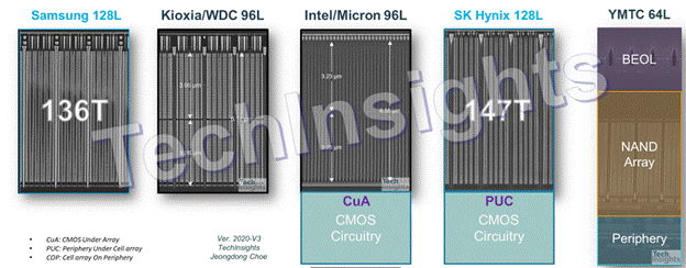
The public tends to focus on layer count, which can be a bit misleading because the actual amount of wordlines – active layers with memory cells – can vary significantly. Other layers can be utilized as dummy wordlines, for example, which help alleviate issues stemming from high layer counts. One measure of efficiency is the total number of layered wordlines divided by total layers, and by this measurement, Samsung has one of the best designs. Samsung is also not using multiple decks or stacks – not “string stacking” as seen with current flash from other manufacturers.
One way to improve overall efficiency is to place the CMOS or control circuitry, generally known as peripheral circuitry, underneath the flash layers. This is known by multiple names such as CMOS-under-Array (CuA), Periphery-Under-Cell (PUC), or Cell-On-Periphery (COP). YMTC’s design is a bit of an exception as it has some circuitry on top of the flash instead, the CMOS being made in a much larger process node before being bonded to the flash. Choe says this technique has potential but currently suffers from yield issues.
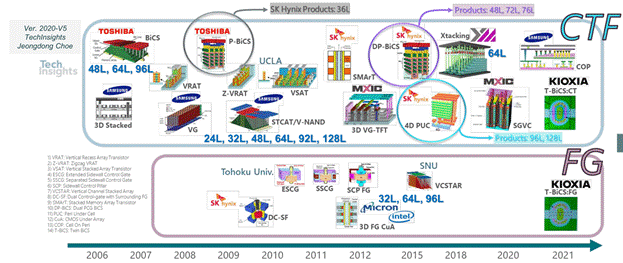
Choe also outlined the history of 3D NAND architecture along with the charge trap flash (CTF) and floating gate (FG) split – Intel and Micron used floating gate, up until Micron’s switch to replacement gate (RG) with its recently-announced 176-Layer flash, while other manufacturers rely on charge trap. Differences here can impact endurance and reliability, scalability, and other aspects of the flash, although Intel’s QLC has benefitted from using floating gate as it maintains better performance with wear.
Kioxia’s future split-gate or split-cell technology is also interesting – it can double density directly and has the benefit of improved endurance due to the semi-circular shape of the split-cell, which is particularly robust with a floating gate. Choe anticipates that layer count will continue to rise with an increasing amount of decks or stacks – currently, two is the maximum – with a corresponding increase in the amount of storage per flash die. Choe feels that this, along with other techniques, like Through-Silicon-Via (TSV), Package-on-Package (PoP/PoPoP), and the move to 5LC/PLC, point to 500+ layers and 3-terabit dies within the next decade.
In his second presentation, Choe detailed how cutting-edge flash often makes its way into mobile and embedded products first – phones (“5G”), for example, are a large driver of demand. He also noted that 2D/planar flash is still used for some niche applications – often as low latency SLC as a storage class memory (SCM) alternative to 3D XPoint as found in Optane or Micron’s recently announced X100 – although it is generally no longer seen in the consumer market.
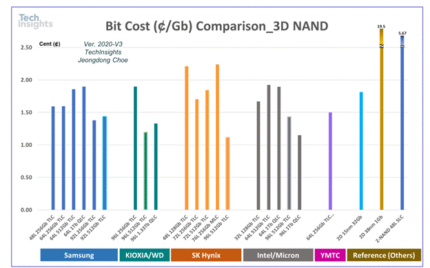
More importantly, he detailed the cost of flash at cent/GB which demonstrates the trend towards cheaper 3D flash while specialized 2D remains many times more expensive. Regardless, the 1xx-layer generation is upon us, as seen with the already released SK hynix 128L Gold P31 and Samsung 128L 980 PRO, Micron’s recent 176L announcement with flash that’s shown up on Phison E18-based drive prototypes, and knowledge that BiCS5 from WD/Kioxia is expected next year along with 144L from Intel for their QLC products. Superior controller implementations will be able to leverage higher flash densities making for faster, more capacious drives in the years to come.
