Intel says defect density at 18A is 'healthy,' potential clients are lining up
Defect density of Intel's 18A seems to be competitive.

Intel this week revealed defect density metrics for its 18A (1.8nm-class) process technology and said that it was healthy at the Deutsche Bank's 2024 Technology Conference. The company also said that the number of customers potentially interested in using this production node was growing.
"I am happy to update the audience that that we are now, for this production process, we are now below 0.4 d0 defect density, this is now a healthy process," said Pat Gelsinger, chief executive of Intel, at the technology conference.
When it comes to defect density (D0), then it is commonly believed that a defect density below 0.5 defects per square centimeter is good (0.5 def/cm^2), so Intel 18A's 0.4 defects per cm^2 is a good result (at least on paper), especially considering the fact that the production technology is a few quarters away from entering mass production, at which point defect density will likely get lower.
Article continues belowIt should be noted that this defect metrics can vary depending on process technology and applications. For example, defect density of TSMC's N7 and N5 process technologies was approximately 0.33 def/cm^2 three quarters before mass production, which is about the same point where Intel's 18A is today.
TSMC's N5 entered mass production with a 0.1 def/cm^2, according to a slide from the foundry published several years ago. N3's defect density was higher than N5's when it entered mass production, but it matched D0 of N5 in five or six quarters (i.e., the improvement curve of N3 matched that of N5 at the same time of their development, this does not mean that D0 of N3 and N5 are the same today).
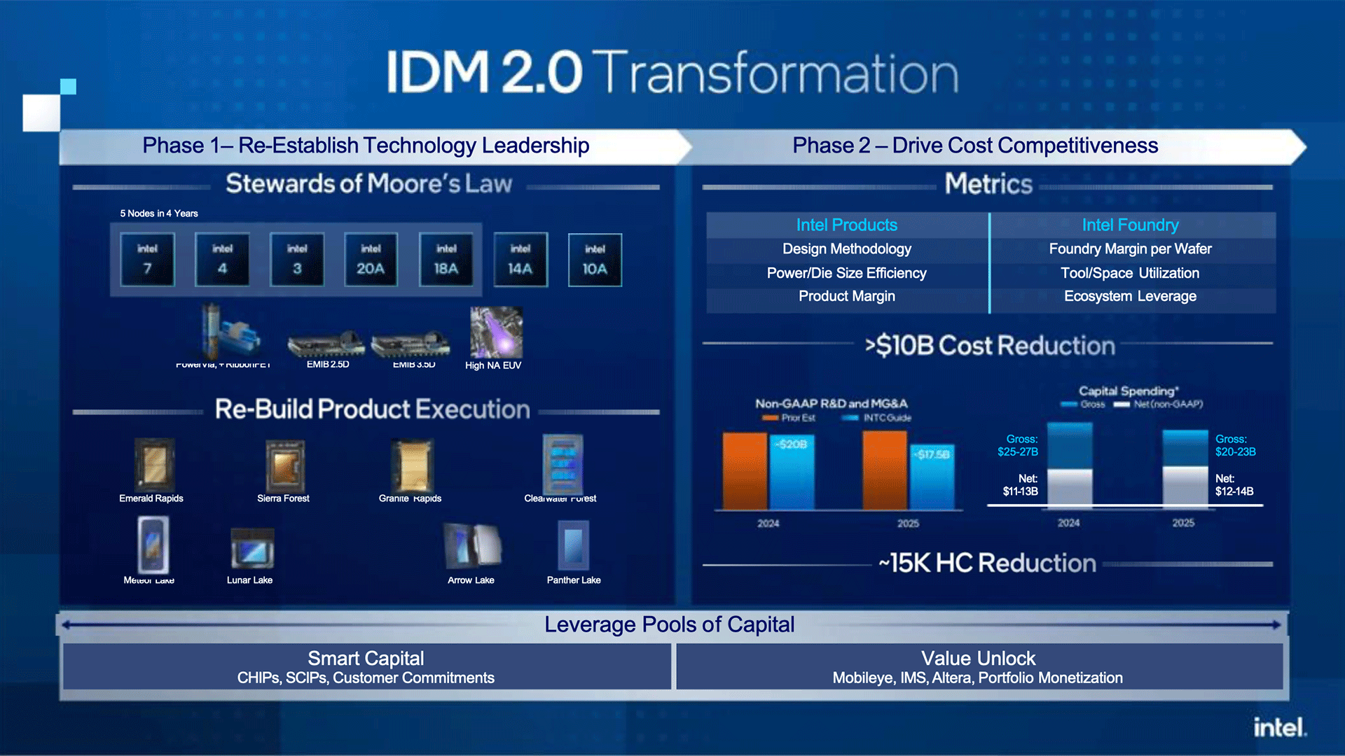
Intel's own first products to use its 18A process technology will be the codenamed Panther Lake processor for client PCs and the Clearwater Forest processor for datacenters. Also, Intel's codenamed Diamond Rapids CPU is also set to use this node. Among external customers, Microsoft confirmed plans to use for a processor and the U.S. Department of Defense is set to use it for its chips. In total, Intel expects eight 18A tape-ins by mid-2025, including internal and external products.
Several weeks ago, Intel said it had released process development kit (PDK) 1.0 for its 18A node, which enables its own developers and customers to start or finalize their 18A chip designs.
Get Tom's Hardware's best news and in-depth reviews, straight to your inbox.
"We now have a dozen of customers that are actively engaged with us around that 18A PDK," Gelsinger said. "We have eight product tape-ins that we expect to finish by the middle of next year."

Anton Shilov is a contributing writer at Tom’s Hardware. Over the past couple of decades, he has covered everything from CPUs and GPUs to supercomputers and from modern process technologies and latest fab tools to high-tech industry trends.
-
Pierce2623 Well maybe the foundry can save the design house from all their screw ups. The last thing we need is less competition in the market.Reply -
watzupken Wow, "lining up". I think we will see if there is a queue lining up indeed. Lining up to test and actual customers are not the same.Reply -
ThomasKinsley I like Intel. I even like Gelsinger, but it's not a good sign when the CEO starts cheerleading future products to regain public confidence.Reply -
Marlin1975 Funny intel says this yet companies that would use it are saying...Reply
"Broadcom reportedly disappointed with Intel 18A process technology — spokesperson confirms evaluation is still in process"
Intel needs to spend less on PR and more on manufacturing side. -
ToBeGood One thing that I really don't understand is that if that is really the case, why Intel can't product, accept the loss and move on? The loss (increase of) of 10%-20% COGS for the next 6 months and 10%-15% (for next 12 months) is totally acceptable (or Not?)?Reply
Even there is no density improvement (with BSPD the improvement alone is 6%), with Meteor Lake Compute Tile i.e. 8.9mm * 8.3mm
https://en.wikipedia.org/wiki/Meteor_Lake
Using the calculator
https://isine.com/resources/die-yield-calculator/
The Yield of D0 < 0.4 (as per Intel statement) for 18A then the Yield is 75%, from TSMC or other Foundry experience, each 3 months there is a 0.1 improvement on average, and if the pattern is follow through, I don't understand why Intel can't produce, that just equal to 10-20% GP disadvantage.
One thing I don't really understand is that Intel 20A/18A is at the level of TSMC A16, for the past couple of years, TSMC increase on average 30% for each generation, from now the N3E to A16, TSMC around 1.7 times (i.e. 1.3 * 1.3 (2 generation est i.e. N2 -> A16), even cost of an N3E wafer is 50% (cost of 20A is 2 times) of 20A, the performance gain of 2 generations, meant that 20A is around 30% more then TSMC with a 2 years advantage, a price that Intel should paid.
Because the PR statement is under Investor Relation site (IR), and the current news is that the shareholder wants to have a class action towards Intel for the Foundry Business, I have no reason that Intel PR / IR will release scientific number in terms of D0 while that is remotely false, since that is already on a possible legal proceedings, any false claim can lead to jail terms.
In fact, the most worry bit is like intel trying to milk the user again, they know that Zen 5 is in trouble (from Microsoft), they know that Lunar Lake is totally on par with Zen 5, they try not to release all the performance possible and let competition and users suffer.
