Samsung's new roadmap unveils its 2nm process nodes and outlines backside power delivery plans
Samsung renames SF3P to SF2 due to better performance, power, and density.

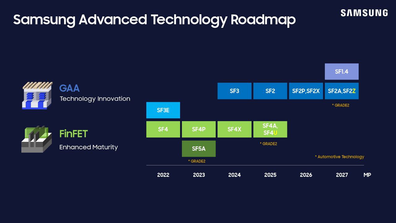
Samsung Foundry has unveiled its new roadmap for chipmaking process technologies at the Samsung Foundry Forum (SFF) U.S. During the forum it outlined plans for 2nm-class nodes, a 1.4-nm-class node, and production technologies with backside power delivery that will be available to its customers in the next three years.
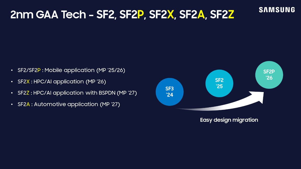
In 2025, Samsung will launch its SF2 node, previously known as SF3P, which demonstrated power, performance, and area (PPA) which the company attributes to 2nm-class process technologies. This manufacturing process is designed primarily for high-performance computing and smartphone applications and therefore Samsung pins a lot of hopes on it. Also, having a 2nm-class node in 2025 formally puts Samsung ahead of TSMC, which will start making chips on its N2 process only in late 2025. Yet, this renaming once again highlights that nanometers hardly matter today.
The following year, in 2026, Samsung plans to introduce SF2P, a performance-enhanced version of SF2 (one might call it SF3P+?). This node will further refine SF2, featuring faster but less dense transistors, indicating a shift towards improving speed while reducing density a little, which is a normal tradeoff in the industry
In 2027, Samsung will release SF2Z, which will incorporate backside power delivery, something that will enable it to improve performance and increase transistor density. In addition, this enhancement aims to improve power quality and manage voltage drops (IR drop) addressing a critical challenge in the production of advanced chips.
Also scheduled for 2027 is Samsung Foundry's SF1.4 node, marking the company's entry into the 1.4nm-class. Unlike SF2Z, SF1.4 will not include backside power delivery, setting Samsung apart from its industry peers Intel and TSMC, which will introduce backside power delivery with their 2nm-class (20A) and 1.6nm-class (A16) nodes. It is unclear why Samsung decided to omit backside power delivery network (BSPDN) with its SF1.4, but it is possible that the company wanted to make this production node a bit more cost-effective.
Samsung's roadmap is now more or less aligned with industry standards concerning 'nanometer' classifications. However, the company has yet to disclose specific performance benefits and comparisons with previous nodes or competitors like Intel Foundry and TSMC.
In addition to the introduction of its high-end nodes, Samsung also unveiled its SF4U, a cost-effective variant of its 4nm-class nodes that enhances power, performance, and area (PPA) through optical shrink. SF4U mass production is set for 2025.
Get Tom's Hardware's best news and in-depth reviews, straight to your inbox.
Overall, Samsung's announcements highlight the company's continued efforts to refine and improve semiconductor process technologies every year. Introducing features like backside power delivery and various performance enhancements promises to make Samsung Foundry competitive with its rivals in the coming years. However, the lack of details in the announcement raises more questions than answers.

Anton Shilov is a contributing writer at Tom’s Hardware. Over the past couple of decades, he has covered everything from CPUs and GPUs to supercomputers and from modern process technologies and latest fab tools to high-tech industry trends.
-
user7007 well hopefully that's true. because my understanding is the tsmc iphone chips were better and the tmsc nvidia chips were better when compared apples to apples. but it's been a few years, hopefully samsung (and intel) will be competitive.Reply

