TSMC Reveals 2nm Node: 30% More Performance by 2025
TSMC details nanosheet-based GAAFET N2 process node.

Taiwan Semiconductor Manufacturing Co. today officially introduced its N2 (2nm class) manufacturing technology, its first node that will use gate-all-around field-effect transistors (GAAFETs), at its 2022 TSMC Technology Symposium. The new fabrication process will offer a full-now performance and power benefits, but when it comes to transistor density, it will barely impress in 2025 when it comes online.
Being an all-new process technology platform, TSMC's N2 brings in two essential innovations: nanosheet transistors (which is what TSMC calls its GAAFETs) and backside power rail that both serve the same goal of increasing performance-per-watt characteristics of the node. GAA nanosheet transistors feature channels surrounded by gates on all four sides, which reduces leakage; furthermore, their channels can be widened to increase drive current and boost performance or shrunken to minimize power consumption and cost. To feed these nanosheet transistors with enough power and now waste any of it, TSMC's N2 uses backside power delivery, which the foundry considers to be among the best solutions to fight resistances in the back-end-of-line (BEOL).
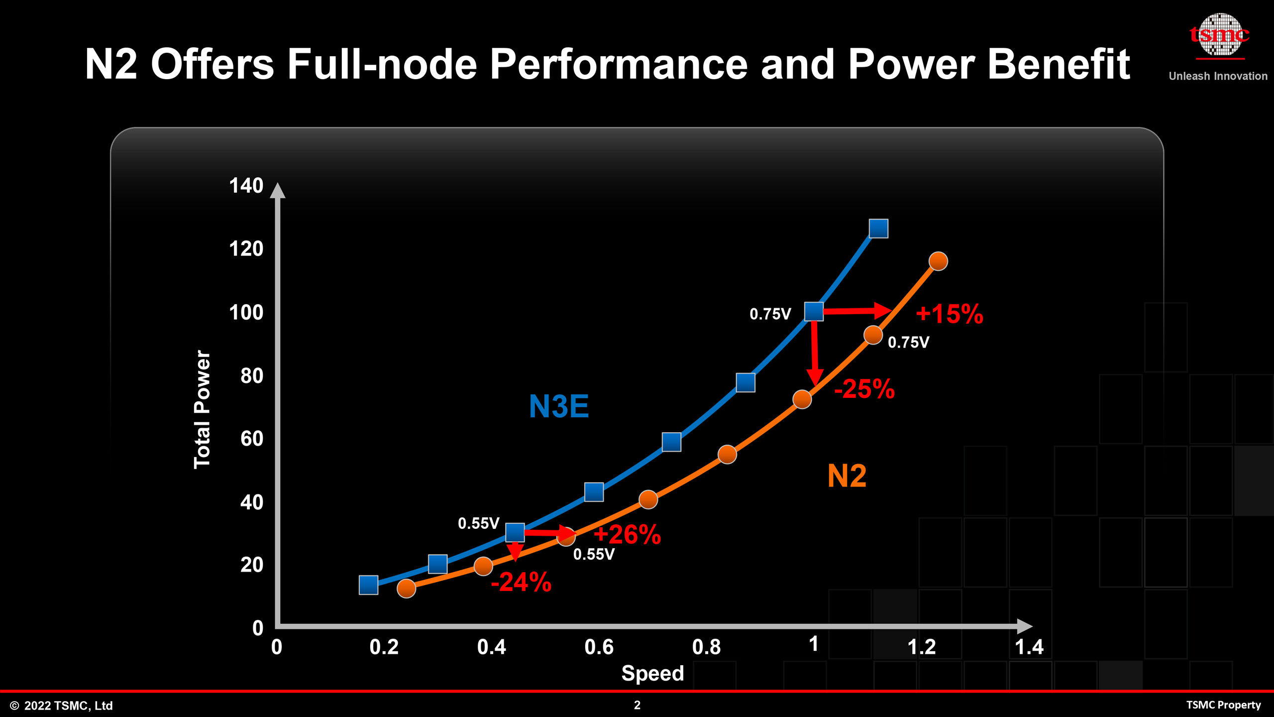
Indeed, when it comes to performance and power consumption, TSMC's nanosheet-based N2 node can boast of a 10% to 15% higher performance at the same power and complexity as well as a 25% to 30% lower power consumption at the same frequency and transistor count when compared to TSMC's N3E. However, the new node increases chip density by only around 1.1X compared to N3E.
| Header Cell - Column 0 | N2 vs N3E | N3E vs N5 | N3 vs N5 | N5 vs N7 |
|---|---|---|---|---|
| Speed Improvement @ Same Power | 10% ~ 15% | +18% | +10% ~ 15% | +15% |
| Power Reduction @ Same Speed | -23% ~ -30% | -34% | -25% ~ -30% | -30% |
| Chip Density | >1.1X | 1.3X | ? | ? |
| HVM Start | H2 2025 | Q2/Q3 2023 | H2 2022 | Q2 2022 |
In general, TSMC's N3 does offer full-node performance increases and power consumption reductions. But density-wise, the new technology can hardly impress. For example, TSMC's N3E node offers a 1.3X chip density increase over N5, which is a substantial increase. For justice, we need to note that TSMC uses somewhat convoluted 'chip density' metrics to describe transistor density on N3E and N2 in its materials published at its 2022 Technology Symposium. Chip density essentially describes a hypothetic chip consisting of 50% logic, 30% SRAM, and 20% analog circuits. Modern designs are very SRAM intensive, but SRAM barely scales, just like analog circuits; hence an N2 chip featuring 50% of circuits that do not scale will demonstrate mediocre scalability compared to an N3E IC. If compared to N3S, a transistor-density optimized version of N3, the result might be even less impressive.
TSMC positions its N2 for various applications, including mobile SoCs, high-performance CPUs, and GPUs. Among the features of the N2 platform (in addition to GAA nanosheet transistors and backside power rail), the world's No.1 foundry mentions 'chiplet integration,' which probably implies that many applications that will use N2 will also use multi-chiplet packages to optimize performance and costs.
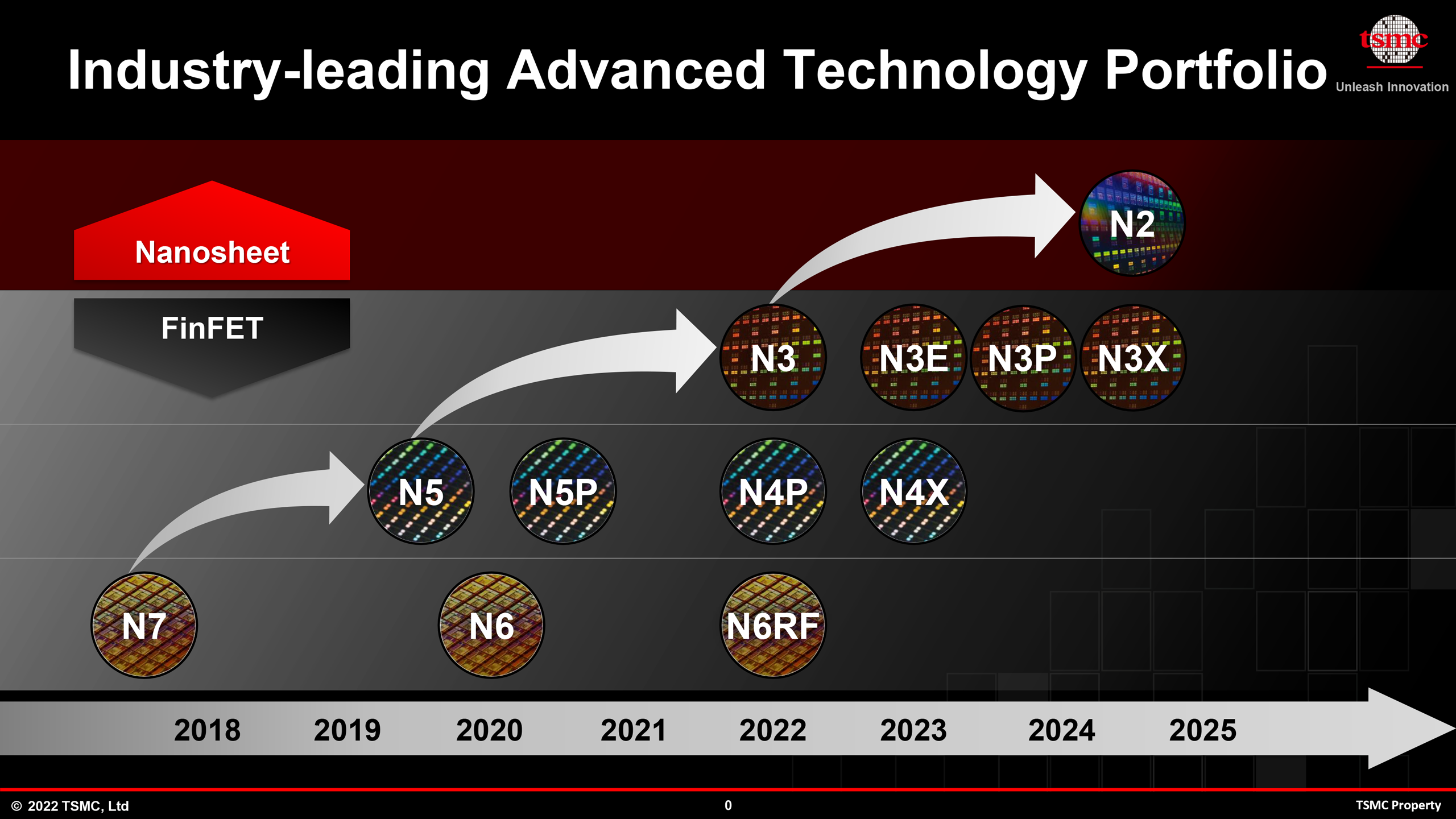
As reported, TSMC will begin high-volume manufacturing of chips using its N2 node in the second half of 2025, so bearing in mind how long contemporary semiconductor production cycles are, expect commercial 2nm chips to emerge on the market only in late 2025 or instead in 2026. Of course, before now and in 2026, TSMC will offer a variety of N3 (3nm class) nodes, but this is a different story.
Get Tom's Hardware's best news and in-depth reviews, straight to your inbox.

Anton Shilov is a contributing writer at Tom’s Hardware. Over the past couple of decades, he has covered everything from CPUs and GPUs to supercomputers and from modern process technologies and latest fab tools to high-tech industry trends.
-
mwestall Did anyone proof read this? Gibberish sentences, spelling errors, grammar issues. Come on guys, get a proofreader.Reply

