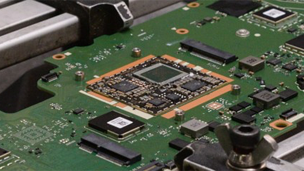
Huawei's 5nm Kirin 9006C laptop chip was reportedly produced by TSMC in 2020, dispelling production rumors at Chinese fab SMIC
No, SMIC hasn't used its own 5nm node for the 9600C.

A recent teardown by TechInsights revealed that Huawei's HiSilicon Kirin 9006C processor used in the Qingyun L540 laptop was made using a 5nm-class process technology. However, it was made by TSMC in Taiwan and not by blacklisted SMIC in mainland China, reports Bloomberg. This finding challenges the assumption that SMIC had developed its own 5nm-class production node for high-volume manufacturing (HVM).
Huawei's HiSilicon Kirin 9006C system-on-chip in the Qingyun L540 laptop was made by TSMC using its 5nm-class process technology and assembled around the third quarter of 2020. This was around the time when U.S. sanctions against Huawei kicked off, according to TechInsights. Analysis reveals that the SoC was packaged during the 35th week of 2020 (August 24 – August 30, 2020), just two weeks before TSMC lost the legal ability to supply chips to Huawei.
As reported several weeks ago, the specifications of the Kirin 9006C SoC are identical to the original HiSilicon Kirin 9000 processor made in 2020. The TechInsights team has concluded that the two processors in question are identical dies fabricated by TSMC. After a detailed examination of the critical dimensions on the die, the researchers confidently affirmed that the HiSilicon Kirin 9006C SoC is produced using TSMC's N5 process technology.
Meanwhile, the newly discovered chip is marked as the 'HiSilicon Hi36A0C GFCV101 JTBFB2U7Q2 2035-CN,' while the one made in 2020 is marked as 'HiSilicon Hi36A0 GFCV101' and the manufacturing date is followed by TW, which points to Taiwan. That said, the Kirin 9006C application processor is likely packaged in China.
Huawei's procurement of this three-year-old processor raises questions about how the company got the silicon. The most obvious answer is that the Chinese giant uses the stock it was aggressively stockpiling in 2019 – 2020 after the U.S. government included Huawei and its subsidiaries into its Entity List in 2019 and then banned exports of all U.S.-originating technologies (which includes chips made using American fab tools) to Huawei. Yet, it is unclear why Huawei did not use the SoC earlier and allowed an expensive piece of silicon to lie unused for over three years.
A domestic 5nm manufacturing technology used for high-volume production would have been a significant achievement for China. Still, it looks like SMIC's alleged N+2 process technology belongs more to the lab than the high-volume fab. Yet, many industry experts are sure that the company will develop a 5nm-class production node and a 3nm-class fabrication process over time.
Get Tom's Hardware's best news and in-depth reviews, straight to your inbox.

Anton Shilov is a contributing writer at Tom’s Hardware. Over the past couple of decades, he has covered everything from CPUs and GPUs to supercomputers and from modern process technologies and latest fab tools to high-tech industry trends.
-
peachpuff Who exactly thought that smic produced it? Anyone with a single brain cell could tell you that was old stock.Reply -
toffty Any and all news from China really should be assumed false from the start until it can be verified.Reply
They have hundreds of chip companies being created to go after the easy money before declaring bankruptcy after the money stops.
I can't blame the companies as they're going after easily swindled money.
This story is a prime example. 5nm production? No. I'd even heavily question anything under 10nm.
Even trying to reverse engineer the manufacturing equipment is very difficult. It'll take another decade for China, and even the US, to be able to have everything that's required to make sub 10nm chips at scale from home-sourced manufacturers.
Chip fabrication is global, requiring hundreds of specialized entities to create the tools, materials, and final product. -
NinoPino Reply
I actually read of it from Tom's Hardware, not from a Chinese news site.toffty said:Any and all news from China really should be assumed false from the start until it can be verified. -
NinoPino "it is unclear why Huawei did not use the SoC earlier and allowed an expensive piece of silicon to lie unused for over three years."Reply
Somebody have a plausible explanation for this ? -
thekingofALLmonkz Reply
They actually did use the 9006C in their QingYun L420, and that was a couple years ago:NinoPino said:"it is unclear why Huawei did not use the SoC earlier and allowed an expensive piece of silicon to lie unused for over three years."
Somebody have a plausible explanation for this ?
https://www.notebookcheck.net/Huawei-Qingyun-L420-with-5-nm-Kirin-9006C-SoC-turns-up-as-the-incoming-successor-to-the-ARM-based-L410-laptop.582694.0.html -
thekingofALLmonkz Reply
Sorry to burst your bubble, but it was already confirmed months ago that SMIC accomplished 7nm on DUV for the Kirin 9000S.toffty said:Even trying to reverse engineer the manufacturing equipment is very difficult. It'll take another decade for China, and even the US, to be able to have everything that's required to make sub 10nm chips at scale from home-sourced manufacturers. -
Darkoverlordofdata Yes, it's mostly tomshardware pushing these rumors. Or should I say 'Hey Anton - you ever check out these stories, or do you just print them?'Reply -
The Historical Fidelity Reply
It is not a viable process with an estimated 15% wafer yield due to the use of DUV quad patterning. The resulting cost of a working die is around 10 times higher than TSMC.thekingofALLmonkz said:Sorry to burst your bubble, but it was already confirmed months ago that SMIC accomplished 7nm on DUV for the Kirin 9000S. -
thekingofALLmonkz Reply
The point is that they made it, regardless of whether it's worth it. It's a huge accomplishment on their part.The Historical Fidelity said:It is not a viable process with an estimated 15% wafer yield due to the use of DUV quad patterning. The resulting cost of a working die is around 10 times higher than TSMC.