SK hynix to spend $90 billion to build 'world's largest mega fab complex' — first fab operational in 2027
The quadruple fab complex is on the way.

SK hynix will begin constructing its mega fab complex called the Yongin Semiconductor Cluster in March 2025, with a completion date estimated in 2046 (via ComputerBase). The complex, which includes four separate fabbing facilities, will cost at least 120 trillion Korean won or just shy of $90 billion. Once completed, it will likely be the largest fab complex in the world, and there's even more room in the broader area for companies like Samsung to build other facilities.
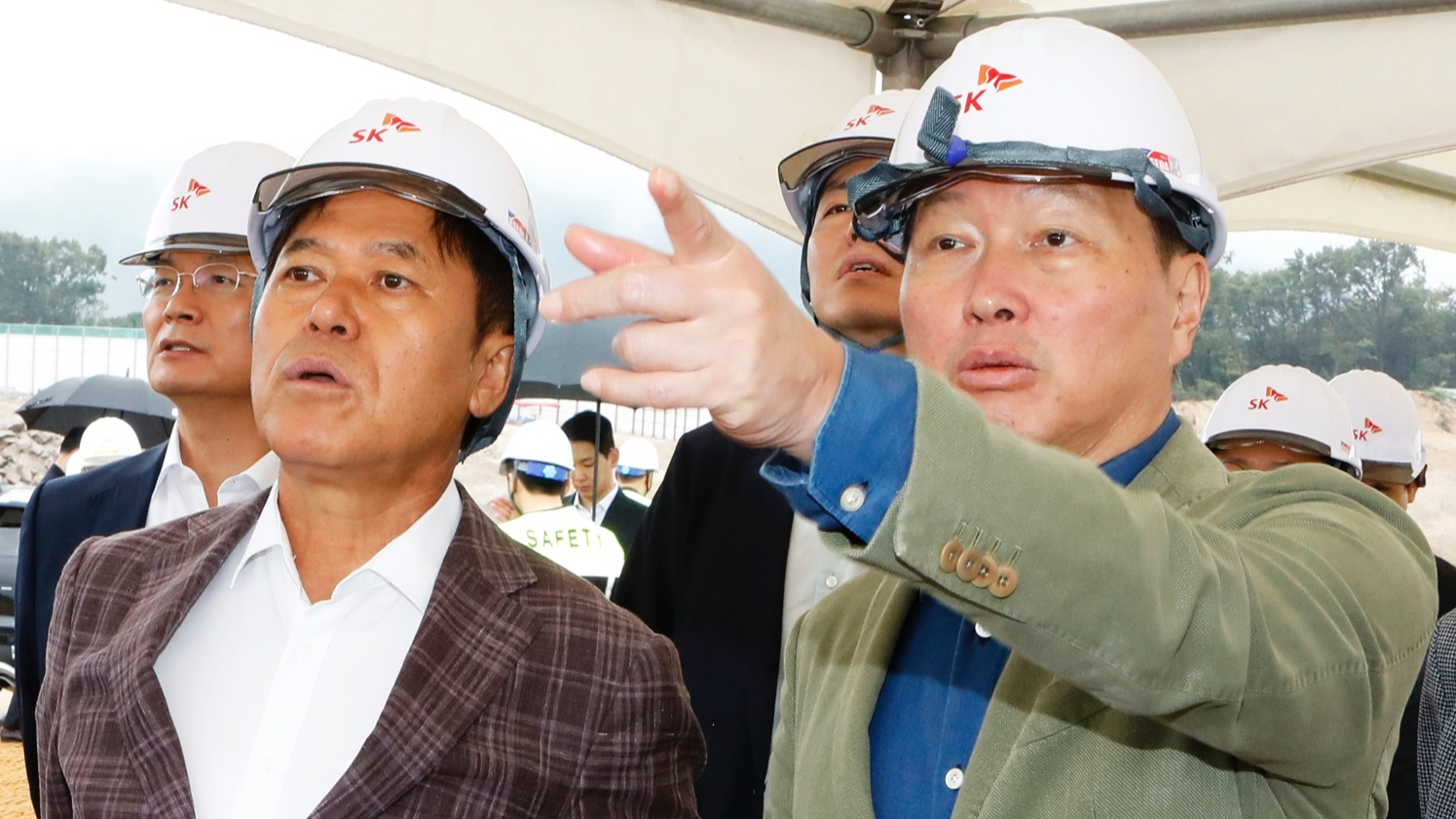
SK hynix, one of South Korea's most notable semiconductor firms, has been planning its quadruple fab complex in the Gyeonggi Province next to Seoul for several years. The construction site is currently being prepared, and apparently, a third of those preparations have been completed, which likely means construction will start as planned in March 2025.
Although the completion date for the entire complex is set for 2046, that doesn't mean individual fabs won't be online before then. Back in September, SK hynix said the first of the four fabs would be completed in 2027, or roughly two years after construction starts. We don't know what will be produced at this first fab, but since SK hynix produces RAM and NAND chips, so it will likely be one of those. HBM may be a prime candidate given the demand for it in server-class and AI-oriented hardware.
If each fab takes two or three years for construction, it raises questions about why the complex will take 19 years instead of somewhere between eight and 12. However, building so many fabs in such a small area may pose unique challenges regarding building support facilities (like water treatment) and logistics. Schematics for the complex show that the four fabs themselves only take up about half of the entire complex, so quite a few other buildings are planned as well.
Once completed in 2046, the mega fab complex will probably be the world's largest, and Fab 1 is also apparently set to be the world's largest three-story fab when it's done in 2027. The wider Gyeonggi area will also host other chip-making facilities from companies like Samsung. SK hynix and Samsung are already envisioning the construction of 13 more fabs and three R&D facilities in Gyeonggi. This project is backed by a $463 billion budget, funded mainly by Samsung and partners.
Get Tom's Hardware's best news and in-depth reviews, straight to your inbox.

Matthew Connatser is a freelancing writer for Tom's Hardware US. He writes articles about CPUs, GPUs, SSDs, and computers in general.
-
Pierce2623 Uhhh guys….we’re clearly buying too much memory/flash if SK Hynix is building the largest fans in the world. The whole AI craze is kinda weird anyways until it does stuff cooler than making bad art and bad articles. The only really cool thing I’ve seen is a guy talked one of the gpt versions into writing him a Gameboy emulator.Reply -
Steve Nord_ Reply
Hah, it misheard plants as fans? I mean, it's consistent for a Chaebol... What's with seemingly confusing long term memory with compute in memory (nominally DDR) and AI?Pierce2623 said:Uhhh guys….we’re clearly buying too much memory/flash if SK Hynix is building the largest fans in the world. The whole AI craze is kinda weird anyways until it does stuff cooler than making bad art and bad articles. The only really cool thing I’ve seen is a guy talked one of the gpt versions into writing him a Gameboy emulator.
You're probs missing the AI article's like the PNNL one on saving 1000 grad student hours doing electron microscopy until the interesting areas of sample are boiled down, or lots of arXiv bits from Netflix DevOps-ish peeps. Or not hunting down the 'less of this, please' buttons in your feed (no longer RSS.)