AMD's $199 RX 6500 XT Restricted to PCIe 4.0 x4
AMD's latest chip presents a lesson in die and cost-cutting measures.
AMD earlier this week introduced the world to its latest GPUs developed around the RDNA2 architecture, the Radeon X 6500 XT and RX 6400. Aimed at entry-level gaming systems, the RX 6500 XT is definitely the more interesting of the two cards, particularly for gamers on a budget. It's essentially the first RDNA2-based GPU targeted towards a sub-$199 price point — the fact that the RX 6400 is only for OEM distribution doesn't help its case here. However, it seems that AMD didn't simply develop a smaller, cut-down GPU, but took cost-cutting measures even further.
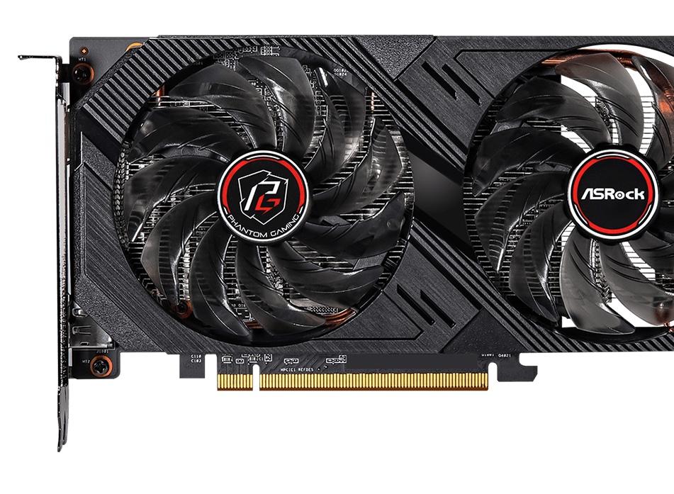
As spotted by Videocardz, ASRock's product page for the RX 6500 XT Phantom Gaming D 4GB OC shows the PCIe bus bandwidth has been halved again compared to the RX 6600 XT, and now only supports a PCIe 4.0 x4 link. This results in AMD's RX 6500 XT having the same PCIe bandwidth available to it as the latest performance-category NVMe SSDs.


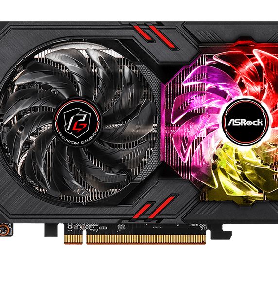
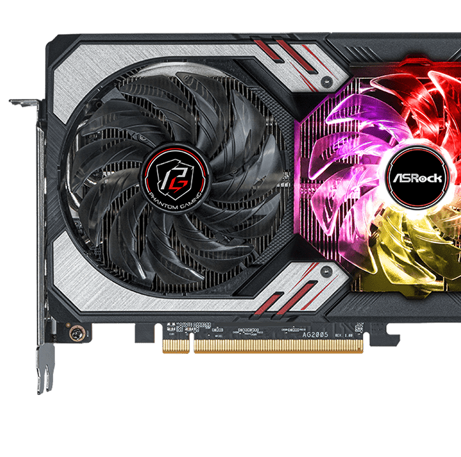
Zoomed images across the PCIe connectors of the RX 6500 XT, RX 6600 XT, and RX 6700 XT showcase the physical differences: the RX 6500 XT capture only shows PCIe traces above up to the x4 link capacity (at the first quarter of the large gold connector). The RX 6600 XT, which we already know uses a PCIe 4.0 x8 link, has traces until the middle of the connector. The RX 6700 XT, utilizing the full PCIe 4.0 x16 link, has traces through the length of the connector.
What might this mean for your gaming experience, you ask? Well, if you're on the latest motherboard with PCIe 4.0 support, not much. The Navi 24 at the heart of the RX 6500 XT has half the computing resources of the RX 6600 XT chip. It's likely the PCIe bandwidth needed to keep the chip fed with data won't be particularly high, and AMD markets the card for 1080p gaming. That resolution doesn't place too much strain on the modern, 8 GB/s bandwidth of the PCIe 4.0 x4 link the RX 6500 XT uses.
But things get trickier if your motherboard was architected for a previous generation PCIe standard. Remember that PCIe is backwards compatible, and plenty of users might still be making do with the older PCIe 3.0 standard (that's about as far as we'd go on this dive down the PCIe support rabbit hole). But that's far enough: Intel only launched CPUs with PCIe 4.0 support with Rocket Lake CPUs less than nine months ago, and we suspect most people running such a CPU will already have a faster graphics card.
The biggest market for a budget GPU like the RX 6500 XT will be older PCs looking for an inexpensive upgrade. That's a lot of potential customers still rocking PCIe 3.0 motherboards, and performance could very much suffer in such scenarios. From there, we still have to filter out those who would be looking to upgrade their graphics card to a $199-class card, but the global numbers on that should be far from negligible.
The RX 6500 XT only uses a PCIe x4 connection, which means bandwidth is now cut down to just 4 GBps on PCIe Gen3. This could present itself as a bottleneck in those systems. Of course, only testing will be able to tell for sure if the bottleneck exists, but one thing is certain: AMD is already saving costs on PCB and trace complexity by opting for a four-lane connection.
Navi 24 loses support for hardware-accelerated AV1 encode and H.264/4K, H.265 decode

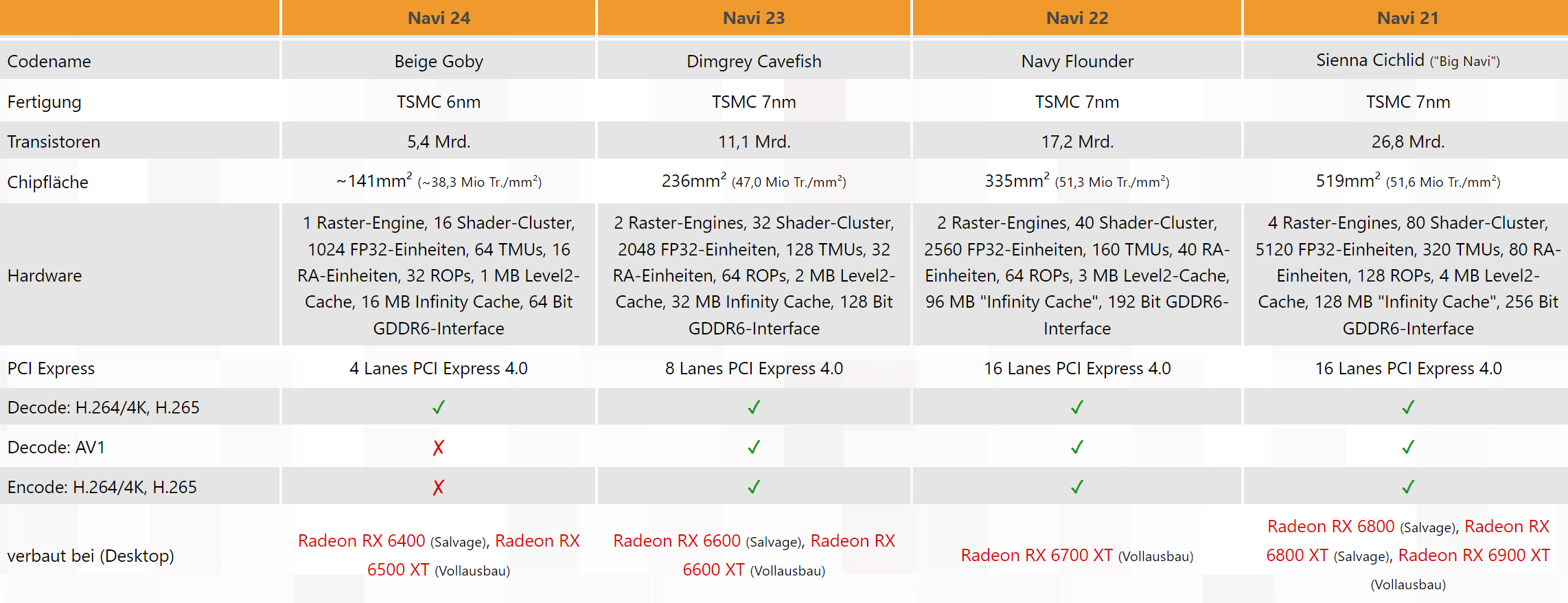
Another decision by AMD is somewhat puzzling, as according to 3D Center, Navi 24 has lost support for hardware-accelerated AV1 decoding, and for H.264/4K, H.265 encode as well. It's a step back from the hardware acceleration found in previous RDNA2 products that did offer those options.
It seems that the Navi 24 chip has received a tinkered-with media acceleration engine that borrows more from Vega's media blocks than from even the original RDNA architecture of the RX 5000-series, which did at least offer H.264/4K, H.265 encode support. Considering that the RX 6500 XT could be the cheapest discrete graphics card available to gamers from the current generation, it will likely be paired with lower-tier CPUs by consumers on a tighter budget, who will be hit hardest by the slower software encode.
Is 6nm a troubled manufacturing process?
It's interesting to look at the RX 6500 XT from a technology and manufacturing process perspective as well. Along with the RX 6400, these are the first two cards built on TSMC's 6nm process. This is a more advanced manufacturing node than the 7nm one that produces some of the world's best graphics cards, including the rest of AMD's RX 6000 series line-up. According to TSMC, the 6nm node leverages more Extreme Ultra Violet (EUV) lithography, and is completely design compatible with 7nm designs, while offering an up to 18% higher transistor density. Interesting, then, that current estimated transistor densities and area improvements for Navi 24 seem to have floated down stream, as we've seen in the previous chart.
We know that higher margins are found in higher-tier products, and with the (never-ending) current state of the market, AMD can sell any GPU it can produce. So this should give us some pause: why wouldn't AMD port the more profitable RX 6800 and RX 6900 cards first? Especially considering that the Navi 21 chips powering them would benefit the most from a transistor density increase, due to their huge 520 mm² footprint. AMD could have launched 6nm versions of the RX 6900 XT and RX 6800 XT, perhaps differentiating them as RX 6950 XT and RX 6850 XT to allow for clear separation of the manufacturing processes.
That AMD didn't choose to do this could have many explanations, but Occam's Razor tells us that the simplest one is usually correct. And perhaps the simplest explanation is that the RX 6500 XT and RX 6400 are much smaller and easier to manufacture chips. The Navi 24 chip powering both cards offers exactly half the graphics processing resources found in the Navi 23-powered RX 6600 XT, even at the same 7nm process, that would place the Navi 24 dies at around 118 mm². subtract the expected density increase of TSMC's 6nm process, and we'd end up with a neat, ~100 mm² Navi 24 chip.
However, the Navi 24 die is currently estimated to measure approximately 141 mm², 41% larger than what some educated napkin math tells us it should be. Granted, it's still a much more palatable die area to contend with than the 520 mm² of Navi 21, particularly if there are troubles in the manufacturing floor. And at the same time, the option for the 6nm process allows AMD to increase supply by tapping into a different semiconductor process.
Get Tom's Hardware's best news and in-depth reviews, straight to your inbox.

Francisco Pires is a freelance news writer for Tom's Hardware with a soft side for quantum computing.