It Begins: Carbon Nanotube Transistors Outperform Silicon In Research Lab
The University of Wisconsin-Madison (UW-Madison) announced that it created carbon nanotube transistors that outperform traditional silicon and gallium arsenide transistors by carrying 1.9x more current. The researchers noted that this is the first time that carbon nanotubes transistors have outpaced silicon. The recent news that carbon nanotube-based memory has moved from the research lab to the production fab is exciting, and if the researchers at UW-Madison have their way, NRAM memory might be accompanied by nanotube-powered CPUs.
The semiconductor industry is encountering numerous challenges as the race to increase transistor density slows and Moore's Law expires. Materials science is becoming increasingly important, because silicon transistors are rapidly approaching the limits of scaling. There is a general consensus that silicon will stop scaling around 5nm, so researchers have been investigating new materials that might replace it.
Carbon nanotubes hold promise, but they have languished in the lab for decades due to economic and technological hurdles. However, the development efforts are moving forward, and Fujitsu announced last week that it is licensing Nantero's CMOS-based carbon nanotube processing technology to move its NRAM memory into mass production in 2018. Carbon nanotube CPUs and GPUs might be a bit further out on the timeline, but recent advances indicate they might be coming sooner than we think.
How It's Done
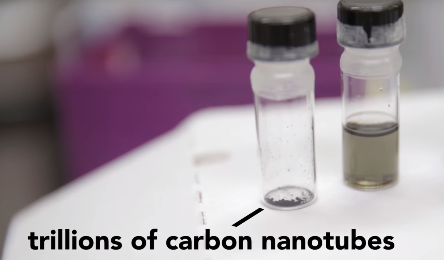
Carbon nanotubes consist of sheets of carbon (one atom thick) that are rolled into tubes that measure between 1nm and 2nm in diameter. Carbon nanotubes are one of the most electrically conductive materials known to man, and researchers contend that a single carbon nanotube can perform five times faster, and with five times less energy, than a normal silicon transistor.
The nanotube performance measurements are impressive, but filtering out impurities at such a small scale is challenging; even a single metallic impurity can severely restrict performance--sort of like short-circuiting the nanotube. The researchers created a new technique that uses polymers to filter out the impurities. The process creates a good base material with "less than 0.1 percent metallic nanotubes."
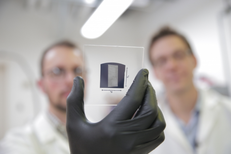
The next challenge is to arrange the tiny nanotubes uniformly into cohesive arrays, so the researchers devised a new "floating evaporative self-assembly" technique that allows them to align the nanotubes on a 1 x 1-inch wafer. The current fabrication technology will require more development to become applicable to larger (and thus economically viable) wafers. However, the beginning efforts are promising; the team noted that its scalable deposition process coated the wafer in less than five minutes.
The polymers that the scientists use to align the carbon nanotubes form a barrier between the tubes and the electrodes (interconnects), so the researchers bake the finished array in a vacuum oven to remove the polymer. The team claims to have achieved "excellent electrical contacts to the nanotubes."
Get Tom's Hardware's best news and in-depth reviews, straight to your inbox.
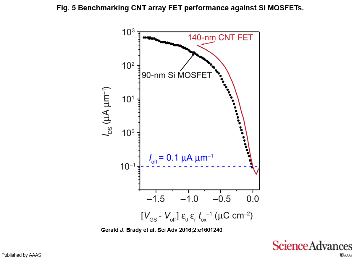
Finally, the team pitted its 140nm carbon nanotube transistor against a 90nm silicon P-channel MOSFET and recorded a 1.9x increase in current. It's notable that the scientists chose a 90nm MOSFET due to its similar size, geometry and leakage current. The carbon nanotube FET had the disadvantage of a larger node and still fared well, but the results do little to illustrate performance against current 14nm FinFET or Tri-Gate transistors.
But Is It Viable?
Carbon nanotubes have been the darling of the research lab for seemingly forever, but it appears that several breakthroughs are finally occurring in parallel. The Nantero/Fujitsu carbon nanotube memory fabrication process uses standard CMOS manufacturing technology, which reduces the amount of investment required to spin up a new fab. Unfortunately, the biggest hurdle for carbon nanotube transistors will come in the form of the expensive R&D and fab equipment needed for mass production, which might keep carbon nanotube transistors in the lab for another few years.
Intel presented a slide at the ISC 2016 Conference in Frankfurt, Germany, that outlined the current challenges facing the semiconductor industry as Moore's Law and Dennard Scaling expire. As the slide noted, power consumption, clock frequency and thread performance all plateaued in 2010. Transistor density isn't far behind. The projected end of rapid advances is expected to be ~2020, which highlights that silicon is fast approaching its limits. There are several other initiatives underway, such as quantum computing, but we shouldn't expect those to emerge anytime soon.
Perhaps carbon nanotubes will be the new tech that rides in to save the day, but the demonstration is far from a completed project. The speed of a single nanotube is five times faster than a silicon transistor, but surrounding structures, such as performance-killing interconnects, might slow them down. As we mentioned in the recent Kaby Lake launch, interconnects (and the insulators) are becoming more of a challenge as lithographies shrink.
A modern chip has 8 to 15 layers of sandwiched interconnects that connect the transistors. The tiny interconnect filaments are copper, which loses the ability to carry current as it gets smaller (they are already a few atoms thick). The layers of insulators between the interconnects also reduce performance. In the past, Intel used glass as an insulator between the interconnects, but it recently began to use air (an excellent dielectric), to boost performance. Additional advances in interconnect technology will likely help unlock the true performance of the underlying carbon nanotubes.
The UW-Madison researchers published a paper outlining the process in Science Advances, but if you don't have a Ph.D. in materials science, it might be a bit much to decipher. The researchers patented the new technology through the Wisconsin Alumni Research Foundation but did not make any predictions about when it will make its way to market.

Paul Alcorn is the Editor-in-Chief for Tom's Hardware US. He also writes news and reviews on CPUs, storage, and enterprise hardware.
-
AndrewJacksonZA "but if you don't have a Ph.D. in materials science, it might be a bit much to decipher."Reply
Hey, Gordon Freeman only has a Ph.D. in Theoretical Physics and he worked in the Anomalous Materials department without any issue, so I don't think a person needs a Ph.D in materials science specifically. -
DavidC1 BTW, there's no such thing as a wonder material. It comes from decades of hard work. In the 1980s, they report only using handful of materials from the periodic table for computer chips. In the 1990s, 2-3 more. Now, they have to use 60% of the elements known in the periodic table of elements to make CPUs.Reply
Real limits are coming.
Also there's a bigger issue than computer chips that allow you to watch youtube videos and post more facebook updates. That's health. Nanotechnologies have the capability of surpassing cellular barriers that create cancer and other dangerous health issues. Carbon Nanotubes and Graphene specifically.
Of course, scientists play with the world and deal with the after effects later. -
Jarmund Really interesting article, i'm always excited to see new technologies being developed to increase computing power.Reply -
turkey3_scratch This is fascinating, but still can't go below 1 atom, so while this may end up prolonging the ever-coming death the chip progress, it still won't keep it going that long. As far as carbon is concerned, diamonds are just carbon, those don't seem to harm people's health.Reply -
Paul Alcorn Reply18554858 said:"but if you don't have a Ph.D. in materials science, it might be a bit much to decipher."
Hey, Gordon Freeman only has a Ph.D. in Theoretical Physics and he worked in the Anomalous Materials department without any issue, so I don't think a person needs a Ph.D in materials science specifically.
I stand corrected :P


