Fujitsu To Mass-Produce NRAM Carbon Nanotube Memory In 2018
Fujitsu announced that it has licensed Nantero's carbon nanotube-based NRAM (Non-volatile RAM) and will participate in a joint development effort to bring a 256Mb 55nm product to market in 2018. Carbon nanotubes are a promising technology projected to make an appearance in numerous applications, largely due to their incredible characteristics, which include unmatchable performance, durability and extreme temperature tolerance. Most view carbon nanotubes as a technology far off on the horizon, but Nantero has had working prototypes for several years.
The battle for the future of non-volatile memory is heating up, as numerous products, such as 3D XPoint, work their way to market. Carbon nanotubes feature their own unique blend of attributes that may just outstrip them all if the price is right. I have to admit, the thought of a carbon nanotube SSD is enticing. Let's take a closer look.
The Particulars
NRAM is a flexible technology that vendors can use to produce memory or storage products. The real attraction of carbon nanotubes begins with their DRAM speeds, but unlike DRAM, the material retains stored data after the power source is removed. The material itself switches between states in picoseconds (a trillionth of a second), but the DRAM interface limits performance to the nanosecond range (>5ns).
Article continues belowThe "persistent" capability mirrors that of other emerging technologies, such as 3D XPoint, ReRAM and PCM, but NRAM purportedly features higher performance than the competition. Other products also suffer limited endurance thresholds, whereas Nantero's NRAM has been tested up to 10^12 (1 trillion) cycles. The company stopped testing endurance at that point, so the upper bounds remain undefined. It is safe to assume that endurance is essentially unlimited for most practical, and even impractical, applications.
Heat tolerance factors into any endurance equation, but NRAM can withstand temperatures up to 800 degrees C, though the company has only tested the current version at 200 degrees C during an active state (fulfilling data requests). The spec noted that NRAM retains stored data for more than 1,000 years at 85 degrees C and more than 10 years at 300 degrees C.
How It Works
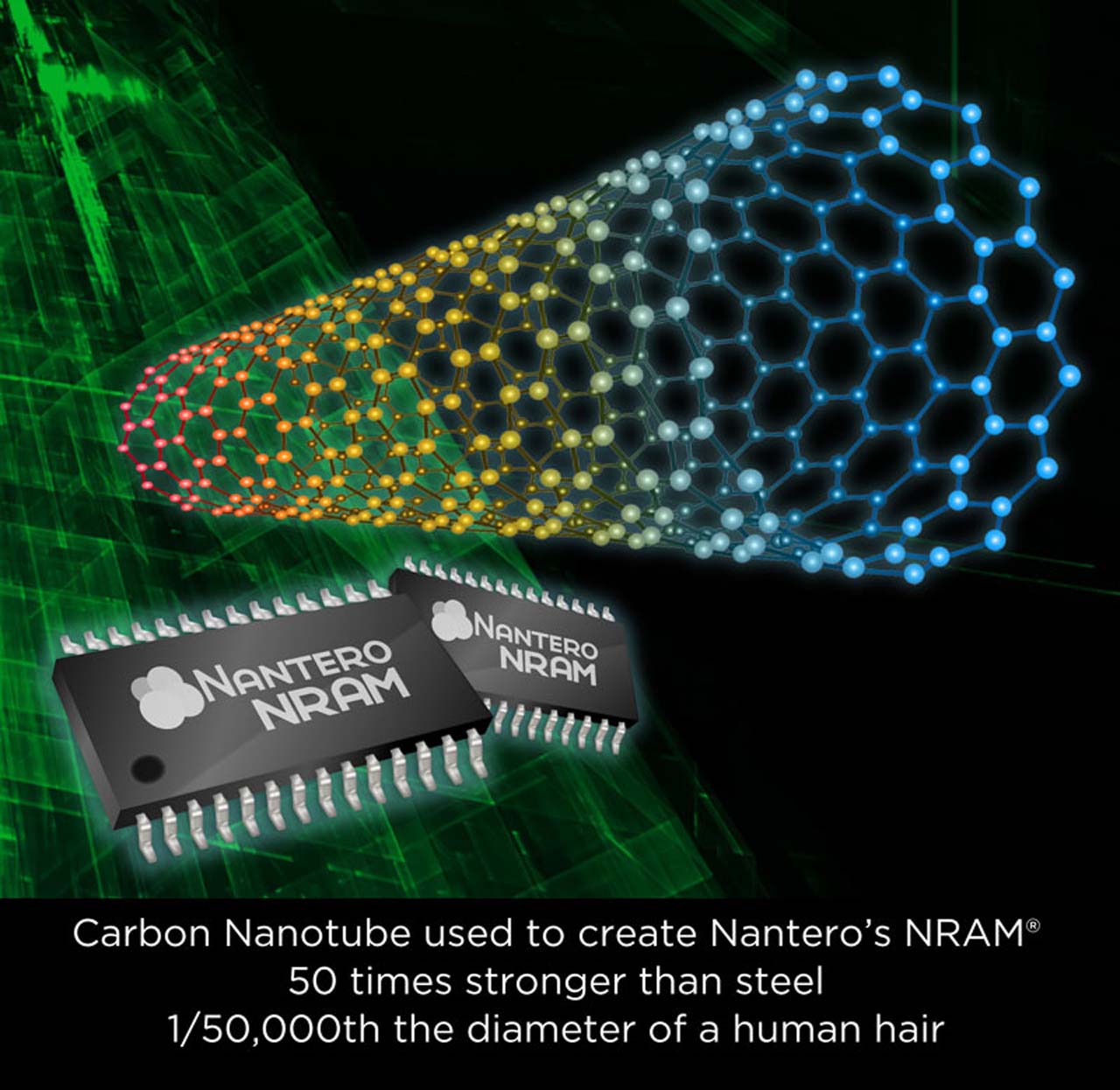
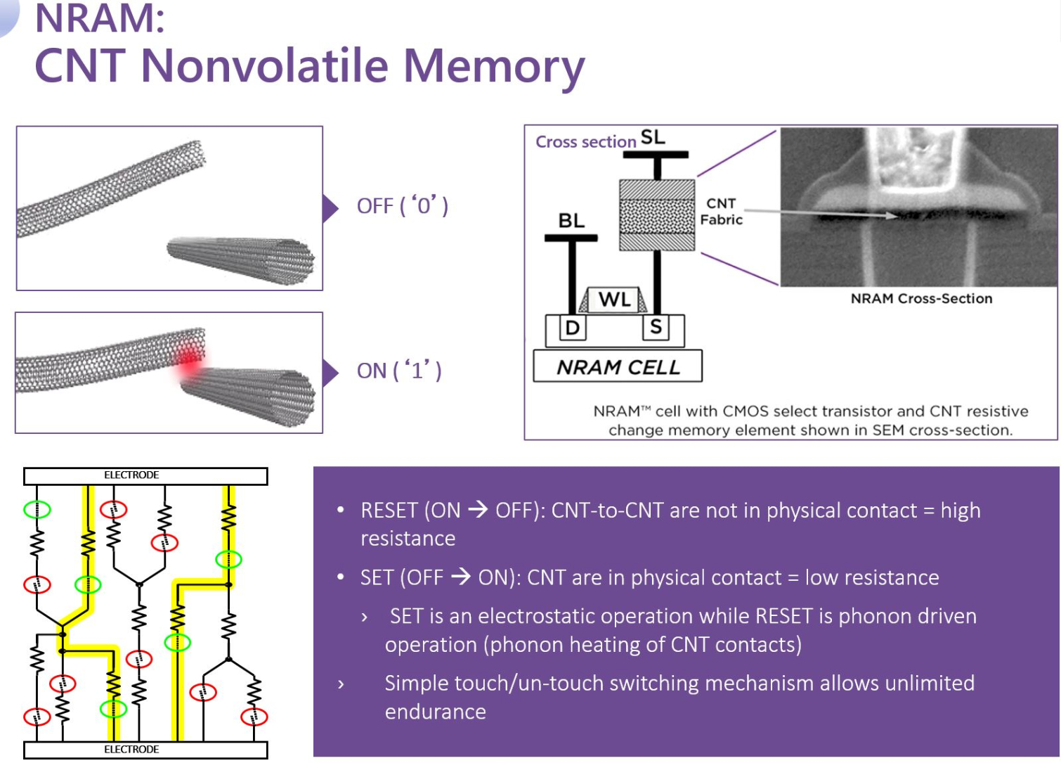
The NRAM carbon nanotubes are 2nm in diameter. Much like NAND, fabs arrange the material into separate cells. NAND employs electrons to denote the binary value held in each cell (1 or 0), and the smallest lithographies hold roughly a dozen electrons per cell. NRAM employs several hundred carbon nanotubes per cell, and the tubes either attract or repel each other with the application of an electrical current, which signifies an "on" or "off" state. NRAM erases (resets) the cells with a phonon-driven technique that forces the nanotubes to vibrate and separate from each other. NRAM triggers the reset process by reversing the current, and it is reportedly more power efficient than competing memories (particularly at idle, where it requires no power at all).
The technology currently stores one bit per cell. However, varying the voltage causes some groups of nanotubes (within each cell) to touch each other, while others will not come into contact. This presents the capability to support multiple bits per cell (similar to MLC and TLC NAND), which increases density. Nantero also sees a path forward with vertical 3D arrangements. Much like NAND, NRAM can scale density through lithography shrinks (it projects sub-5nm) or 3D multi-layered architectures. Fabs can also stack NRAM die with wire bonding and TSV techniques to create high-density packages.
Get Tom's Hardware's best news and in-depth reviews, straight to your inbox.
Spinning The Silicon
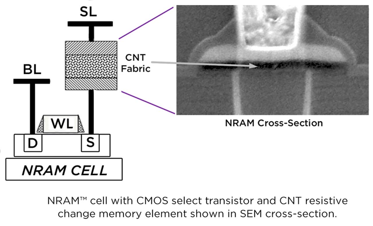
The technology is amazingly simple to produce. It's merely a thin layer of carbon nanotubes that are spin-coated onto a normal wafer and then sandwiched between two layers of interconnects. The interconnects use a crosspoint implementation. Unlike NAND, which has to erase cells in large blocks, NRAM is bit-addressable. The ability to program and erase each bit separately provides tremendous performance and allows it to operate as either memory or storage. The products communicate through the DDR4 interface, which actually constrains the performance of the underlying media, but it could theoretically communicate through other protocols, such as NVMe, as well.
The manufacturing process employs normal lithography and etching techniques on standard CMOS wafers. In fact, Nantero claims to be the only company with a patented (175+ and counting) CMOS-compatible process. The easy CMOS manufacturing technique doesn't require expensive re-tooling, which leaps the economic hurdles that prevent many promising technologies from making it to market.
The Path To Market
Fujitsu is just the first company to announce that it's producing the technology. Nantero claimed that it is working with six other (unannounced) fabs, and some are already developing 28nm 3D designs that enable "multi-GB" products that are denser than DRAM. Nantero indicated that its partners will announce these products soon. The company also has 12 other (unspecified) customers in place, but because Nantero merely licenses the technology to others, it cannot provide details.
The extreme endurance and heat tolerance makes the new technology very promising for embedded caches on SoCs and processors. Numerous other applications require extreme temperature tolerances, such as components used in oil and gas drill heads. Unsurprisingly, Schlumberger, one of the largest oil and gas exploration companies, has invested heavily in the technology.
Nantero, which began its work in 2001, has produced several working prototypes and rocketed the technology into space on a 2009 space shuttle Atlantis mission. An independent third-party lab has already tested its products, which lends credence to Nantero's claims.
Keys To Success
Pricing is always the key ingredient to success, and Nantero indicated that the leading-edge products will ship with half the cost of DRAM, and prices will fall as production ramps and the vendors shrink lithographies and stack layers. Increased density will also allow the technology to penetrate a broader range of applications.
Intel's and Micron's (IMFT) competing 3D XPoint technology is much closer to market, but pricing remains hazy, and it will require expensive new production techniques and tools, which doesn't help. Also, 3D XPoint is a "captive" technology that will be unique to the IMFT alliance, whereas Nantero is more than happy to license its technology to a range of fabs. It's doubtful that NRAM would be a serious competitor to 3D XPoint in the short term, but considering that 3D XPoint isn't even on the market yet and also faces significant pricing challenges, it could be a threat over the coming years.
The important takeaway is that carbon nanotube products have busted out of the research lab and into production fabs. The early products will focus on highly specialized applications, such as embedded caches and storage-class memory applications. If the price is right, the technology will trickle down into more familiar devices, such as SSDs, in the future.

Paul Alcorn is the Editor-in-Chief for Tom's Hardware US. He also writes news and reviews on CPUs, storage, and enterprise hardware.
-
Wow, so these are physical switches that turn on and off, as the tubes jump up and down? Crazy. It just sucks that initial chips will be 32 MB ones.Reply
-
bit_user This is awesome! Thanks for breaking it down for us, Paul!Reply
I wonder if these chips are sensitive to static electricity (not ESD, but just the static electric field), in a fashion similar to how magnetic storage is sensitive to magnets. Hard drives are pretty safe, in their metal cases, which are a natural consequence of their various mechanical constraints. But, if NRAM ships in some kind of DIMM or M.2 form factor, then will they have to essentially wrap them in foil to protect the data from accidental erasure?
-
WFang The article states "will ship with half the cost of DRAM" but ends with "If the price is right, the technology will trickle down into more familiar devices, such as SSDs, in the future."Reply
If first gen ships with prices 'half the cost of dram', would that not imply that the price is 'right' straight of the bat? -
hdmark Reply18530661 said:The article states "will ship with half the cost of DRAM" but ends with "If the price is right, the technology will trickle down into more familiar devices, such as SSDs, in the future."
If first gen ships with prices 'half the cost of dram', would that not imply that the price is 'right' straight of the bat?
i could be wrong.. but i think what hes saying is if it starts at half the cost of DRAM (16gb for 100$ for ddr4? so 16gb NRAM for 50$) then hopefully it will drop more to SSD pricing eventually (250gb for 100$)
either way this is great and im excited!
*fixed my typo :P* -
WFang Replyi could be wrong.. but i think what hes saying is if it starts at half the cost of DRAM (16gb for 100$ for ddr4? so 16gb NRAM for 100$) then hopefully it will drop more to SSD pricing eventually (250gb for 100$)
Ah, yes, I could see that, except I think you have your numbers wrong ;) If 16GiB DRAM is $100 and this NRAM is half, it would be $50 for 16GiB NRAM.. but yeah, its quite a bit more than what we pay for SSD drives for sure.. Your post, and my giant cup of coffee made that pretty clear! :P
either way this is great and im excited!
So yeah, as a high activity hot-swap type disk, a smaller disk with 1000+X endurance and less power for same performance would still be valuable in enterprise, but not so much for normal home use where SSD endurance is less of a problem currently, but storage space IS important.
Definitely exciting, and perhaps we won't have to wait too long to learn more: "some are already developing 28nm 3D designs that enable "multi-GB" products that are denser than DRAM. Nantero indicated that its partners will announce these products soon."
If mechanical disk and SSD paired to make hybrids, perhaps we'll see hybrid SSD+NRAM in the next few years as well? Done correctly, you could probably achieve higher reliability/endurance on an SSD if you had e.g. 32GiB of NRAM to use for data that changes frequently, and the SSD is more of an archival dump. -
ComputerSecurityGuy I am thinking it will hit the cache/mobile market soon. I wouldn't be surprised to see new lines of Qualcomm Snapdragon chips that support it as an option, and even chips by various companies that use it as an on package cache. Think about an extra 256MB cache, relatively inexpensive and with near DRAM performance on the same package as every CPU with an iGPU. Even those that don't. Inexpensive and could make a big difference. And on the flip side an inexpensive and efficient mobile RAM. LPDDR5 perhaps.Reply -
jasonkaler So lets get this right. It's...Reply
Faster than DRAM, - possibly faster than CPU cache
More heat tolerant than just about anything
Longer life than any current SSD technology, with permanent storage
Can be produced in current CMOS fabs
"DDR4 interface...constrains the performance " so it will have much higher timings.
This all sounds too good to be true. It's like Wonderwoman and Superman had a memory baby together. -
problematiq Reply
I suspect price and density will be the first two hurdles. I am actually way more hyped about this than the Xpoint. (was super hyped about Xpoint)18531103 said:So lets get this right. It's...
Faster than DRAM, - possibly faster than CPU cache
More heat tolerant than just about anything
Longer life than any current SSD technology, with permanent storage
Can be produced in current CMOS fabs
"DDR4 interface...constrains the performance " so it will have much higher timings.
This all sounds too good to be true. It's like Wonderwoman and Superman had a memory baby together.
I expect this will be very attractive for data centers if they can up the density.
also.. "Sorry sir the server melted into a puddle of metal, But on the plus side the data is still intact!" -
Discorama LOL sure,Reply
In 2006 (maybe it was 4) Samsung was going to mass produce their 42" organic TVs. Also, there should be like 10 battery technologies in mass production by now that are better than lithium. Most comparatively, in 2014, HP was going to mass produce their cross-bar memory and cross-bar is far simpler to make than these carbon nanotubes sound.
I'll eat my hat if I see any nanotube product in 2019.


