AMD's Thunderbird finally fully fledged
Introduction
Finally the latest trend of the x86-processor arena has caught up with AMD's flagship the Athlon-processor as well. Since Intel had started to integrate 128 kB of second level cache onto the processor die of its Celeron processor (the good old 'Mendocino'-core) late 1998, one processor after the other followed this example. Number two was 'Dixon', Intel's mobile Pentium II CPU with 256 kB L2 cache, then AMD followed with the K6-3 which also sported 256 kB of on-die L2-cache. Finally, Intel launched the famous 'Coppermine'-core, which again uses 256 kB on-die L2-cache to make sure that Pentium III is able to compete with AMD's Athlon CPU. Now AMD followed suit and launched a new Athlon processor, coming with the highly anticipated 'Thunderbird' core.
On-Die Second Level Cache Makes The Difference
What's the big deal about an L2-cache that shares its silicon with the processor core? There are actually several big advantages that make this solution very attractive, but at the same time it's not quite that easy to implement.
On-Die L2-Cache Runs Faster
The first advantage of an L2-cache that is on the same silicon chip as the processor core is the fact that both parts can run at the same clock specifications. This means that the core and the second level cache clock frequency can be identical, making sure that the core doesn't have to wait a long time until the L2-cache delivers data. Before, when second level cache was found on external chips, it was only able to run at half or even less speed than the processor core. The worst scenario was or still is found in Athlon CPUs that run at 900, 950 or 1000 MHz, where the L2-cache is actually clocked at only a third of the core clock, forcing the processor core to wait up to 2 clock cycles until it can receive data from the L2-cache. The 3rd-party SRAM-makers simply couldn't supply L2-cache modules that would endure more than 400 MHz clock frequency, and so the great Giga-Athlon came so far with an L2-cache that is hardly faster than the L2-cache of an Athlon 800. On-die L2-cache is able to make sure that processors can still receive data from their L2-caches without much wait, even when they run at clock speeds way beyond 1 GHz.
On-Die L2-Cache Should Be Better Connected
The next great advantage of an on-die L2 is the data path between core and L2-cache. External L2-cache modules need to be connected to the processor core, and the wider the data path between the two, the more pins are required of both components. A processor chip has to stick to a reasonable amount of pins though, which restricted external L2-caches to a data path width of only 64-bit. You can imagine that those pin-restrictions don't exactly apply to on-die L2. Here the width of the data path is completely up to the CPU-designers and they will try to make this path as wide as possible. Intel widened the connection between CPU core and the L2-cache of the Pentium III 'Coppermine'-core to 256 bit (part of Intel's 'Advance Transfer Cache'-architecture), which meant a fourfold increase in data bandwidth between CPU core and L2-cache over the previous 'Katmai'-architecture. Unfortunately AMD's engineers were either not willing or not able to fulfill the same task with Thunderbird, so that AMD's new processor is still forced to use a 'one-lane' instead of Coppermine's 'four-lane' road for the data transport between its core and its on-die L2-cache.
On-Die L2-Cache Makes Processors Nice And Small
Get Tom's Hardware's best news and in-depth reviews, straight to your inbox.
Advantage number three doesn't have anything to do with performance, but it's just as important as well. Most of you can certainly remember the times when Intel introduced 'Slot1' and the 'single-edge-cartridge' 'SEC'. This 'awkward' package was necessary to host a printed circuit board (PCB) with the CPU-core chip as well as the external L2-cache modules. Once the L2-cache is integrated onto the same piece of silicon ('die') as the processor core, there's no need for the 'cartridge solution' as used by 'Slot1' or 'SlotA' anymore. This is the reason why the trend goes back to the cheaper and easier to implement PGA (pin grid array) -solutions. For Intel this means going away from 'Slot1' over to 'Socket370' and for AMD the 'SlotA' will be replaced by 'SocketA'. This new standard is a socket with 462 pins and it means the birth of another new connector-version for x86-processors.
All in all it's pretty obvious, an L2-cache integrated on the processor die is basically able to improve its performance and reduce system costs at the same time. In case of Intel's move from 'Katmai' to 'Coppermine' we could see a speed increase up to 10%, as you can read in the article about Coppermine .
The downside of an on-die L2 is the fact that it's not quite that easy to integrate all the millions of transistors into the processor die. Cache needs a lot of silicon and a lot of power. The on-die-L2 cores of 'Mendocino', 'Dixon' and K6-3 were still manufactured in 0.25 micron process, but only the step to 0.18 micron process makes on-die L2 really attractive.
Thunderbird's Specifications
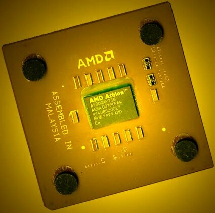
Now AMD managed to equip its Athlon-core with 256 kB on-die and full-speed L2-cache as well, coming with all the goodies discussed above. The new core has received the modest name 'Thunderbird', but the actual product will follow Intel's example of the Pentium III move from Katmai and Coppermine. 'Thunderbird' will still be sold as 'Athlon Processor', but it will be easier to distinguish the 'new' one from the 'old' one, because the 'Thunderbird-Athlon' comes as 'SocketA'-version, while 'Old-Athlon' will naturally remain for 'SlotA' only.
I tried to summarize the differences between Thunderbird and its predecessor in a little table. All the specs that are not listed there should be identical for the two.
| Header Cell - Column 0 | 'Old' Athlon | 'Thunderbird' Athlon |
|---|---|---|
| Manufacturing process | 0.25 / 0.18 micron,Aluminum Interconnect | 0.18 micron,Aluminum / Copper Interconnect |
| Die Size | 102 mm² (.18 micron) | 117 mm² |
| Number of Transistors / Die | 22 million | 37 million |
| Voltage | 1.6 - 1.8 V | 1.7 V |
| Thermal Power at 1 GHz | 65 W | 54 W |
| Maximum Current at 1 GHz | 37 A | 33.6 A |
| L2-CacheLocation | External | On-Die |
| L2-Cache Clock | 33 / 40 / 50 % of core Clock | 100% of Core Clock |
| L2-Cache Size | 512 kB | 256 kB |
| L2-Cache Data Path | 64-bit wide | 64-bit wide |
| L2-Cache Organization | 2-way set associative | 16-way set associative |
| Package | SlotA Cartridge | SocketA 'CPGA'SlotA Cartridge (OEM only) |
| Chipsets | AMD 750AMD 760VIA Apollo KX133 | AMD 750AMD 760VIA Apollo KX133 (questionable stability)VIA Apollo KT133 |
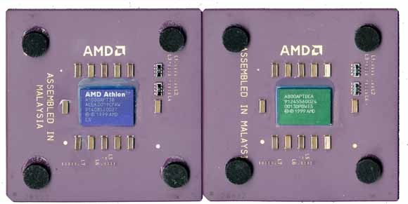
You can see that Thunderbird is still requiring a lot of power and current, so the ones of you who hoped that Thunderbird wouldn't need a power supply as strong as 'old' Athlon might be a bit disappointed. You can also see that there will be two different versions of Thunderbird. One is using aluminum interconnects and will be produced in Fab25 in Austin, the other is using the modern copper interconnect process and will be produced in Fab30 in Dresden. Currently it remains unclear if there will be any difference between the two, besides the different color. Chips with aluminum interconnect seem to have a green shine to them, while the copper-chips look rather blue.
Thunderbird's Specifications, Continued
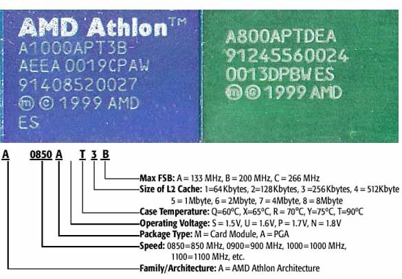
We've tried to decipher the new codes of Thunderbird, as you can see in this picture:
The benchmarks below suggest that AMD made a few more enhancements to the core, but unfortunately we haven't got any detailed information yet what in particular has been changed in Thunderbird's processor core over the old Athlon core.
Overclockers won't be too happy about the fact that Thunderbird is of course multiplier-locked. Goldfinger devices won't help, unless you should get one of the few SlotA-versions of Thunderbird.
Thunderbird Pricing
What we do know is that Thunderbird is quite a bit cheaper to produce and AMD will therefore be able to offer it at very reasonable prices, particularly if you compare them to Intel's P3-pricing:
| ThunderbirdClock Speed | Price |
|---|---|
| 750 MHz | $319 |
| 800 MHz | $359 |
| 850 MHz | $507 |
| 900 MHz | $589 |
| 950 MHz | $759 |
| 1000 MHz | $990 |


