How Memory Access Works
Information is stored by first separating the memory area into rows and columns. The capacity of the individual chips determines the number of rows and columns per module. When several arrays are combined, they create memory banks.
The chips are actually accessed by means of control signals such as row address strobe (RAS), column address strobe (CAS), write enable (WE), chip select (CS) and several additional commands (DQ). You also need to know something about which row is active in the memory matrix at any given moment.
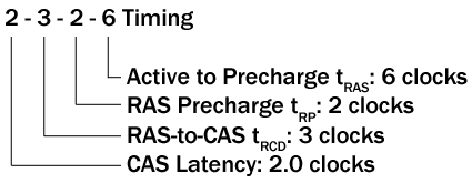
In today's computers, a command rate is defined in BIOS - generally 1-2 cycles. This describes the amount of time it takes for the RAS to be executed after the memory chip has been selected.
The memory controller selects the active row. But before the row will actually become active so that the columns can be accessed, the controller has to wait for 2-3 cycles - tRCD (RAS-to-CAS delay). Then it sends the actual read command, which is also followed by a delay - the CAS latency. For DDR RAM, CAS latency is 2, 2.5 or 3 cycles. Once this time has lapsed, the data will be sent to the DQ pins. After the data has been retrieved, the controller has to deactivate the row again, which is done within tRP (RAS precharge time).
There is one more technical restriction - tRAS (active-to-precharge delay). This is the fewest number of cycles that a row has to be active before it can be deactivated again. 5-8 cycles are about average for tRAS.
Memory timings are generally cited in order of importance: