
We recently got the opportunity to visit one of Micron’s largest and most advanced DRAM manufacturing facilities. The visit impressed us on many levels: the scale of the fab, the advanced manufacturing technologies and techniques being used, and getting to look behind the scenes at the cutting-edge Taichung A3 facility. It was also a great pleasure to meet up with CVP and Head of Micron Taiwan Dr. Donghui Lu, who provided insight into the operations at the enormous ‘One Mega Taiwan’. Last but not least, we learned that Dr. Lu has enjoyed building PC DIY desktops since way back in 1996.

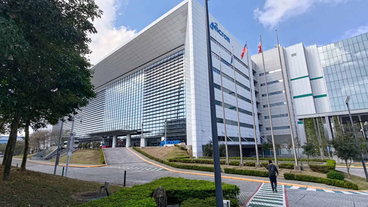

Arriving at Micron Taichung
Houli station, a small provincial stop, is the nearest rail transit link to Micron Taiwan. Emerging from the station you find several bicycle hire businesses outside for people wanting a leisurely ride around nearby parkland. However, around a five-minute taxi ride away is Micron’s colossal Fab 16 which is dedicated to making the world’s most advanced memory chips in Taiwan. Moreover, thousands of people work there (into five figures in the whole of Taiwan), and most need to be highly educated and highly trained for the tasks they do.
There are a lot of huge numbers to take in to weigh up this operation. To sum up the manufacturing facilities here, there are three memory chip production buildings: Taichung A1, A2, and A3. A1 and A2 came to Micron through acquisition, and A3 was the new Fab Micron constructed in 2021. Surrounding these fabs are complementary buildings for the vertically integrated parts of the business – things like MTB (Assembly and Test- backend), TCP (Taiwan Central Probe), and AATT (Advanced Assembly and Testing Taiwan). There are also manufacturing support industries like water, gas, and chemical processing and recycling plants dotted around the fabs.
Micron's newest fabs and buildings utilize sustainable resources and clever recycling. Taichung A3, for example, was constructed in a park with 600 trees. It also uses solar and rainwater resources. It is estimated that Micron's green credentials save 90 million KWh of electricity per year, and 75% of the water used is recycled and reused.
No one wants these fabs to stop due to adverse conditions like drought or power shortages. Thus Micron is aiming for all its Taiwan operations to achieve a 75% reduction in water consumption by 2030, net zero emissions by 2050 using renewable and controlling both direct and indirect emissions. Lastly, Micron Taiwan has already achieved a waste reuse, recycling, and recovery rate of 98.1% in FY23 thanks to its circular economy approach.
What happens at Micron Taichung?
DRAM chips for memory modules are produced in Micron facilities in Taiwan and Japan, with expansion plans announced in Boise, Idaho, and Syracuse, New York. The product portfolio using these memory chips currently ranges from ultra-high bandwidth products like HBM3E through graphics memory like GDDR6X, to LPDDR5 and DDR5 for computers. There are diverse form factors and target markets, too, spanning server, PC, mobile, auto, industrial, HMDs, and AIoT devices. You'll probably be most familiar with Micron DRAM-based products like DDR5 DIMMs and SODIMMs, but the latest LPCAMM2 mobile memory modules will be made by Micron, too.
Dr. Lu explained to us that, in brief, Micron takes in wafers and puts them through its FEOL (Front End of Line), MOL (Middle of Line), memory cell testing, BEOL (Back End of Line), and PROBE (product testing) phases before sending them off to subsequent assembly, test, and packaging steps. Interestingly, the Taichung and Taoyuan fabs work in a unified manner for this operational flow, which Micron dubs ‘One Mega Taiwan.’
The thousands of staff at Micron around the world are involved in activities as diverse as research, electronic design, engineering, product design, manufacturing, product sales, and marketing.
At the time of the visit, Dr. Lu and other Micron execs appeared to be excited by the impending announcement of new HBM3E chips. They even presented us with a commemorative HBM3E memory chip.

Micron executives we met during the visit were clearly energized regarding the prospect of the AI boom delivering an uplift to business. This starkly contrasts with the feeling during last year’s memory industry downturn, almost entirely due to the surge in interest in AI. While 2023 saw the industry take its foot off the accelerator, it takes 9 to 12 months to rebuild production momentum, and this lag is partly why we see the memory business as so cyclical.
The cyclical nature of the business doesn’t affect research, development, and technological refinement. Micron and the other big memory players are well aware that when the cycle turns, they can still benefit from having the best, most advanced memory technologies.


Ahead of SK hynix and Samsung?
Memory making is a highly competitive business, and the three big players are all keen to power the AI revolution. TrendForce notes that, with HMB3E, this will probably be the first time that HBM technology is embraced simultaneously by the power trio.
Micron says that its current memory chips are produced on its 1 alpha and 1 beta processes. 1 alpha process began mass production in Taiwan in 2021. 1 beta memory chips were developed in Japan, but mass production began in Taiwan in 2023. Demand for the current process is outstripping supply, and last year’s downturn is more than partly to blame. Micron uses 1 beta memory chips for its newly announced 24GB HBM3E, which Nvidia has chosen for its H200 GPU accelerators.
In 2025, Micron expects to start producing its 1 gamma memory chip, which was reaffirmed in its Fiscal Q2'2024 earnings call on March 21. 1 gamma will be first ramped in Taiwan and then in Japan. It is already testing this advanced memory, which is fabbed using state-of-the-art EUV machines. Understandably, we weren’t allowed to tour this area of the megafab.
Going forward, it isn’t only things like EUV that will yield benefits. DRAM fabrication, like NAND, will see increased verticality via the use of advanced packaging to boost key properties like performance and density.


What we saw at Micron Fab 16
The two key aspects of Micron’s Taichung operations that we were allowed to view were the Remote Operations Center (ROC) and the showroom at Taichung A3 which provides an expansive view across a fab clean room. Remember, this is where the process of creating the current state-of-the-art 1 beta memory chips on 300mm wafers begins.
Entering the ROC, visitors see a huge mission control area where staff monitors, troubleshoots, and optimizes a process with hundreds of discrete steps, spanning from supplied wafer to finished wafer (a wafer that still needs to be tested, prepared, cut, etc.).
Various data presentation techniques are leveraged in the ROC, with bar charts, color coding, and so on, to make it easily apparent what is happening (and what has recently happened) and highlight anything sub-optimal. Some charts also showed various semiconductor machine brands. The charts and colors made it easy to see an overview and then drill down into anything unusual or not working as expected.
Micron Taiwan is naturally an early adopter of AI in manufacturing, and this is something Dr. Lu is particularly proud of. As part of its smart manufacturing initiative, the firm uses AI and machine learning to accelerate yield ramping and strengthen real-time monitoring. Understanding and interpreting the data on the multitude of screens in the ROC has been improved and accelerated by AI.
Chinese New Year had just passed, but it was strange to see the CNY celebratory decorations in the ROC, as they weren’t red – they were all green. The ROC manager told us that Taiwan’s engineers are averse to red and love green, as a green light on a machine means that all is well. However, we didn’t spot any green packs of Guai Guai around the building.

Taichung A3 viewing
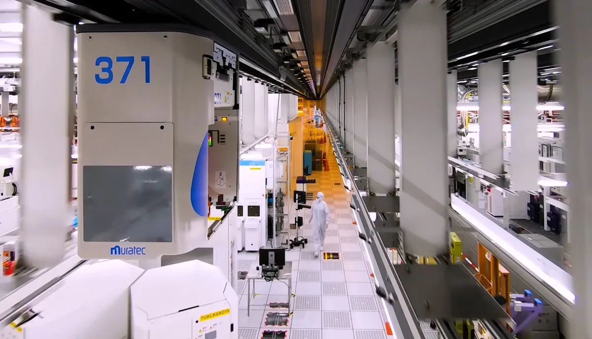
A3 is the newest fab in Taichung, which, unlike the others, has been designed from the ground up by Micron. During our visit to this area of the megafab, the tour started with information about how A3 is as automated as possible to cut down any chance of contamination.
The Taichung A3 clean room we saw from the showroom was full of advanced machinery and Overhead Hoist Transfer (OHT) robots with minimal human intrusions. We constantly saw robots zipping around, each typically holding a large transparent 'AutoPod' caddy. Also important were incredibly clean and constant streams of filtered air and water.
In an earthquake-affected island like Taiwan, readers also won’t be surprised to hear that the machines in the clean room area were all securely attached to the elevated flooring. Dr. Lu told us that some of the processing machinery also featured vibration dampening to shrug off smaller tremors.
Near the end of our visit, we passed through another huge installation at Micron Taichung – the food court. The facility has its own Starbucks, Burger King, 7-11, and various local food outlets for employees on this very high-security site to enjoy during breaks. It was honestly so big that it was difficult to see one end of the rest, food, and drink area from the other.


Executive profile: Dr. Donghui Lu CVP of Front-End Manufacturing and Head of Micron Taiwan
Dr. Lu is the current Head of Micron Taiwan, responsible for manufacturing facilities in Taichung and Taoyuan and aligning the operations on the island to Micron’s global objectives and mission. He’s been at Micron for two years and was our host throughout the tour - from the introduction to Micron Taiwan, accompanying us through to the ROC, and guiding our tour of the Taichung A3 showroom. Dr. Lu has an interesting history in PC tech, and spent 20 years of his career at Intel.
Lu graduated from Tsinghua University in Beijing, China, but went to Ohio State University to further his materials science and engineering studies by completing a PhD. After receiving joint executive MBA degrees in the U.S., Lu worked at Intel for over 20 years. His Intel endeavors spanned technology development and transfer, manufacturing and ramp-up, and fab construction. Lu also played a critical leadership role in growing Intel’s memory business, transferring jointly developed 3D NAND and Optane technology nodes from Micron to Intel.
Dr. Lu is a PC enthusiast and happily recounted his earliest PC DIY memories. He told us that the first desktop PC he remembers building was back in 1996. The system ran Windows NT 3.51 but was updated to NT4 as soon as that came out. Multi-core PCs were not very common back then, but Lu remembers making a dual CPU system in 1997, as his wife wanted a powerful graphics workstation for her work. That dual CPU system used a Tyan motherboard, perhaps the Tyan Tahoe 2 ATX.
Working at Intel might sound like a dream job for PC DIYers. Interestingly, Dr. Lu remembers being allowed to pick up a new CPU for free every year – a nice little perk. For guidance, he would (and assures us he still does) check out Tom’s Hardware component reviews and guides. However, like all of us old-timers lament, he notes that overclocking isn’t the boon it used to be for PC DIYers and tinkerers.
