Join for quick access. Enter your email below and we'll send confirmation plus sign you up to our newsletter.
By submitting your information, you confirm you are aged 16 or over,
have read our
Privacy Policy
and agree to the
Terms & Conditions. Geographical rules apply.
Stay On the Cutting Edge: Get the Tom's Hardware Newsletter
Get Tom's Hardware's best news and in-depth reviews, straight to your inbox.
You are now subscribed
Your newsletter sign-up was successful
Join the club
Get full access to premium articles, exclusive features and a growing list of member rewards.
An account already exists for this email address, please log in.
New technique uses 3D printing to fab three-dimensional chip circuits
Technology can print free-standing metal structures without any support material
Application of the CHARM3D technique to design and fabricate a 3D circuit for a wearable battery-free temperature sensor system, as shown here being worn on a human hand. This demonstrates the great potential of the innovative CHARM3D technique in enabling a wide range of applications in healthcare.(Image credit: NUS News)
The use of 3D circuitry is key in continuing to miniaturize electronics, but it’s been subject to serious drawbacks. The requirement for support materials and external pressure limits how small manufacturers can go, but one research team might have an answer. The engineers have developed a way to build free-standing, self-healing metallic structures without those needs.
Led by Associate Professor Benjamin Tee, the research team from the National University of Singapore (NUS) recently published its findings. Calling its technology CHARM3D, the team demonstrated how it can use 3D metal printing technology to fabricate a wide range of compact electronics, including wearable sensors, wireless communication systems, and electromagnetic metamaterials.
One use the team has identified for its technology is in healthcare. Tee and his team say that CHARM3D allows for the development of vital sign monitoring devices that are completely non-contact. The patient just positions themselves near the sensor, which can detect breathing and other vital signs without ever touching the patient’s skin.
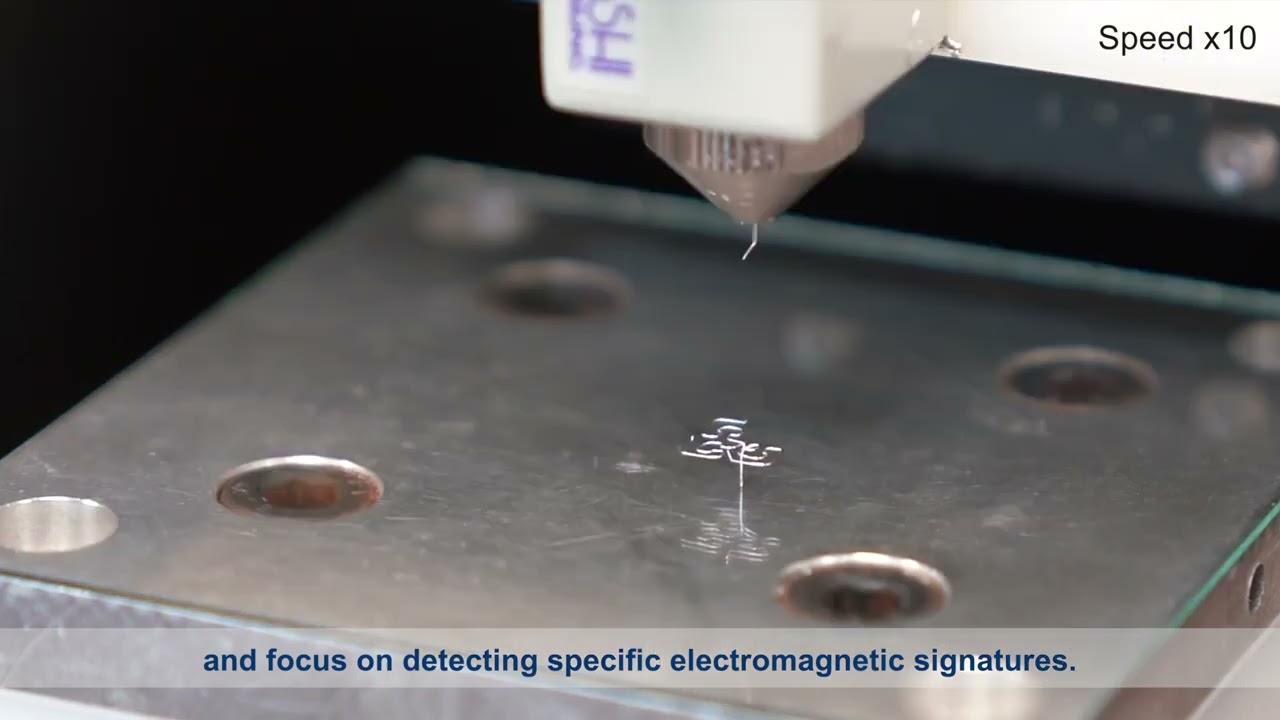
The method uses direct ink writing (DIW), which is already used to fabricate 3D circuits. The challenge has always been that DIW uses materials that aren’t good electrical conductors. That necessitates support materials to hold everything together, limiting what you can achieve.
CHARM3D changes this by incorporating Field’s metal into the technology. Field’s metal is a eutectic alloy of indium, bismuth, and tin and has a rather low melting point for metal. In fact, its melting point is lower than that of the commonly used materials for hobbyist 3D printing, 62º Celsius (143.6º F). It also solidifies rapidly, unlike most composite inks normally used in DIW.
The combination of these characteristics makes Field’s metal an excellent material for direct ink writing three-dimensional circuits. CHARM3D uses it to fabricate highly complex free-standing 3D structures like vertical letters, cubic frameworks, and scalable helixes.
CHARM3D, developed by researchers from the NUS Department of Materials Science and Engineering, is able to print free-standing metallic structures without the need for support materials and external pressure. This new technique fabricates 3D electronic circuits faster and with greater level of detail and accuracy. (Image credit: NUS News)
“By offering a faster and simpler approach to 3D metal printing as a solution for advanced electronic circuit manufacturing, CHARM3D holds immense promise for the industrial-scale production and widespread adoption of intricate 3D electronic circuits,” Tee said.
Stay On the Cutting Edge: Get the Tom's Hardware Newsletter
Get Tom's Hardware's best news and in-depth reviews, straight to your inbox.
Tee’s team also highlights the product's self-healing properties. Since it has a low melting point, the mere application of a heat gun can repair a broken circuit in seconds.
The engineers have already used CHARM3D to fabricate a 3D circuit for a wearable battery-free temperature sensor, antennas for wireless vital sign monitoring, and metamaterials for electromagnetic wave manipulation. The team believes the technology could enable more accurate medical imaging, such as microwave breast cancer imaging to detect tumors earlier. The researchers note that it also holds promise in advanced security applications, such as screening for hidden devices or contraband.
Tee and his team believe they’ve only begun to explore what the technique behind CHARM3D can do and are looking for opportunities to commercialize their work.
Jeff Butts has been covering tech news for more than a decade, and his IT experience predates the internet. Yes, he remembers when 9600 baud was “fast.” He especially enjoys covering DIY and Maker topics, along with anything on the bleeding edge of technology.