AMD Instinct MI200: Dual-GPU Chiplets and 96 TFLOPS FP64
A single MI200 offers nearly 5X the compute of Nvidia's A100
AMD officially revealed its Instinct MI200 compute focused GPU today during its Accelerated Data Center Keynote, delivering a major upgrade over the previous Instinct MI100. The MI200 will be used in the upcoming Frontier supercomputer, powering its exascale performance via thousands of EPYC CPUs and MI200 GPUs. AMD makes numerous comparisons to Nvidia's A100, claiming significant increases in computer performance and density. As always, take these announcements with a grain of salt as paper specs don't tell the whole story, but MI200 looks to be an absolute monster.
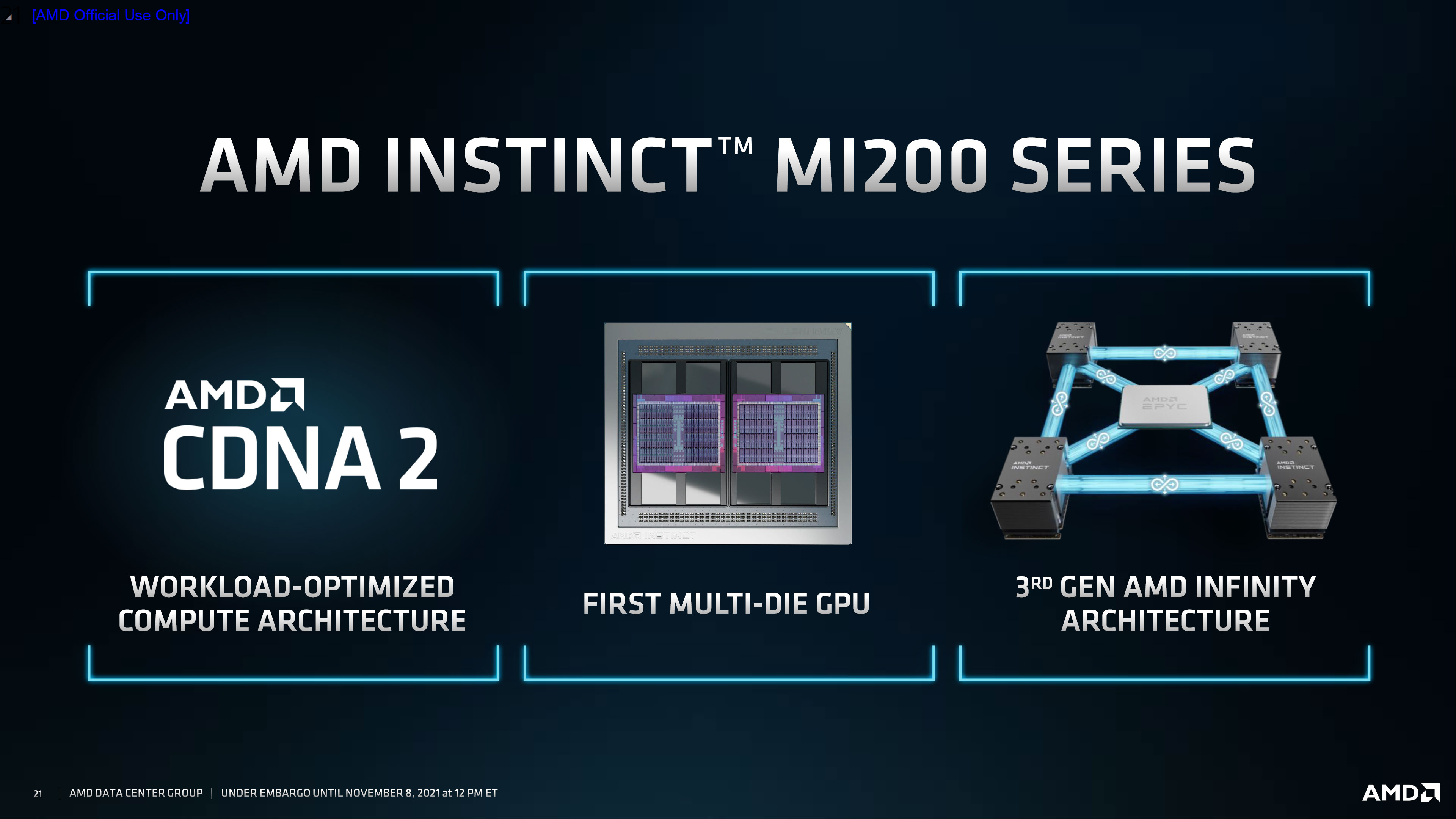
Fundamentally, MI200 appears to use an updated and enhanced version of the GPU that powered the MI100 — AMD calls the architecture CDNA2, similar to the RDNA2 vs. RDNA shift on the consumer side. MI100 had 120 CDNA CUs (compute units) and 7680 streaming processors. MI100 used TSMC's N7 fabrication node, and also supported up to 32GB of HBM2 memory clocked at 1.2 Gbps. MI200 takes the ball and runs with it, boosting all of the key performance metrics.
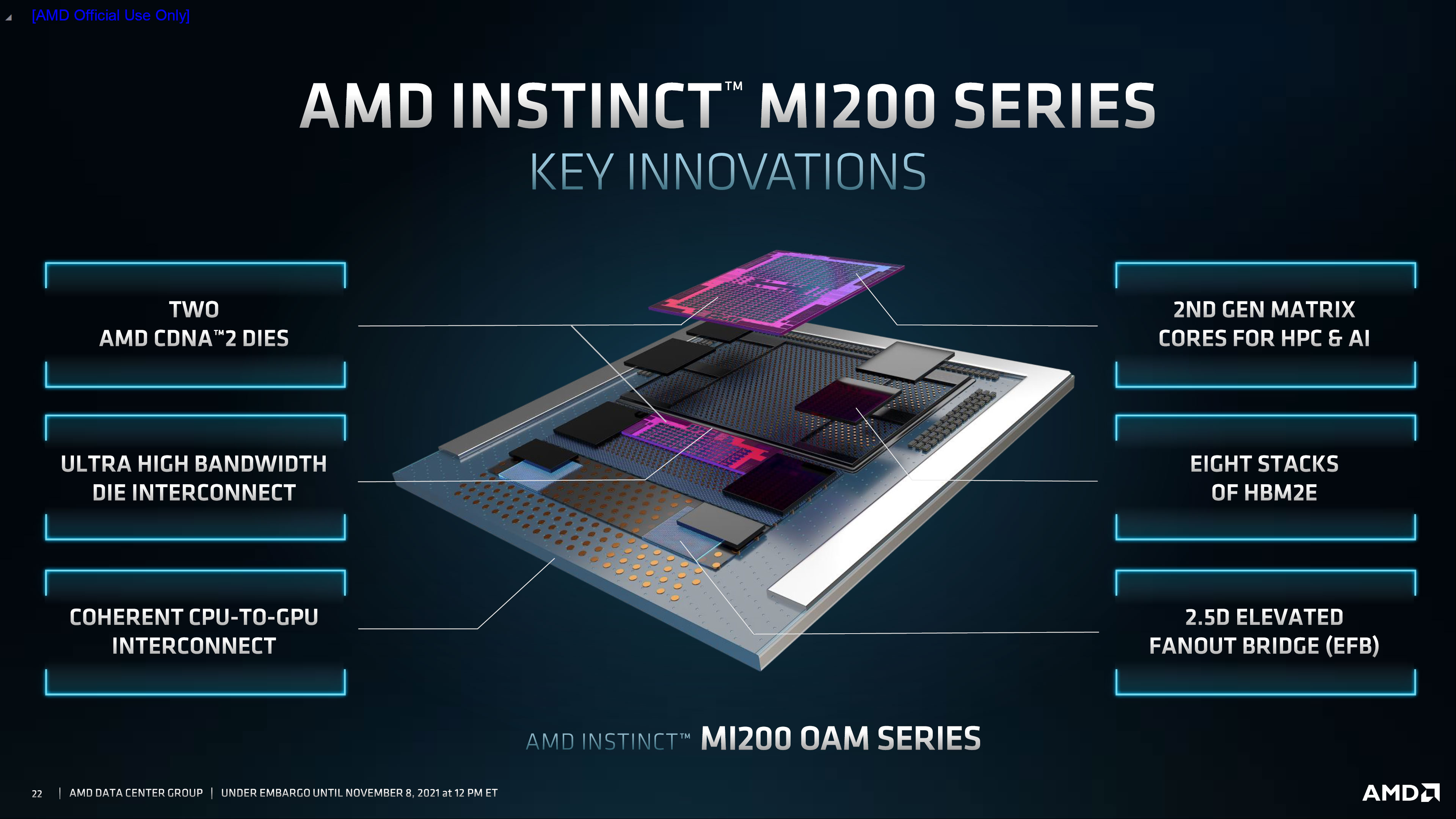
The first major change relative to the MI100 comes in the use of a multi-die package. This is basically taking the same chiplet approach that AMD used in its recent Zen 2 and Zen 3 CPUs and applying that to GPUs, though with some enhancements. The two CDNA dies (that's "Compute DNA", as opposed to the graphics-focused RDNA used in consumer GPUs) are linked together via an Infinity Fabric, with 25 Gbps links providing up to 100 GBps of bi-directional bandwidth between the GPUs. There are eight available links in the MI200 OAM (OCP Accelerator Module, where OCP is "Open Compute Platform") configuration, yielding 800 GBps of bandwidth between the two chiplets.
That's a massive increase over the Infinity Fabric links used in Zen 3, if you're wondering. On Zen 3, the Infinity Fabric operates at the RAM clock, with a maximum official speed of 1600 MHz (though overclocked chips have reached as high as 2000 MHz). With 16 bytes and double data rates, that's only 51.2 GBps of bi-directional bandwidth, meaning MI200 has 16 times the interlink bandwidth. It's AMD's answer to Intel's EMIB, in essence.
MI200 will also use TSMC's N6 node, a refined version of the existing N7. N6 represents a minor evolution in process technology, but it does allow for higher clocks and improved efficiency. It's also compatible with the N7 design rules, meaning it's relatively easy for a company like AMD to port a design from N7 to N6.
One surprising piece of information is that the entire MI200 chip contains up to 58 billion transistors. That's certainly a lot, but Nvidia's A100 by comparison has 54.2 billion transistors in a single GPU core. Unless we've missed something, that means the total size of the MI200 chips are roughly the same size as Nvidia's A100, except they potentially pack a lot more compute performance into that area.
Based on the specifications AMD has released, MI200 will clock at up to 1.7 GHz, compared to 1.5 GHz on the MI100. The memory was also upgrade to HBM2e running at 3.2 Gbps, which combined with the dual-chiplet GPU layout means overall bandwidth for MI200 increased from 1.2 TBps to 3.2 TBps. But that's just getting started.
While many of the core functional units of MI200 appear similar to MI100 — the vector FP64 and FP32 rates look unchanged, along with the matrix FP16 and FP32 rates — AMD has enhanced both the vector and matrix units. Specifically, both matrix and vector computations now have FP64 support, and for the vector FP64, the rate of computation has been doubled.
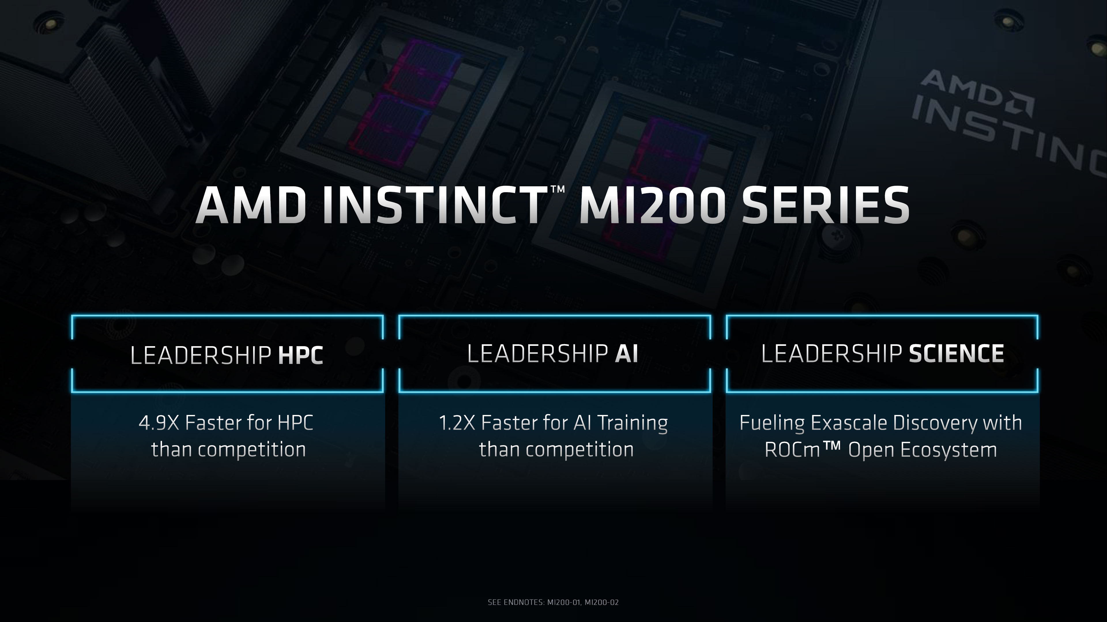
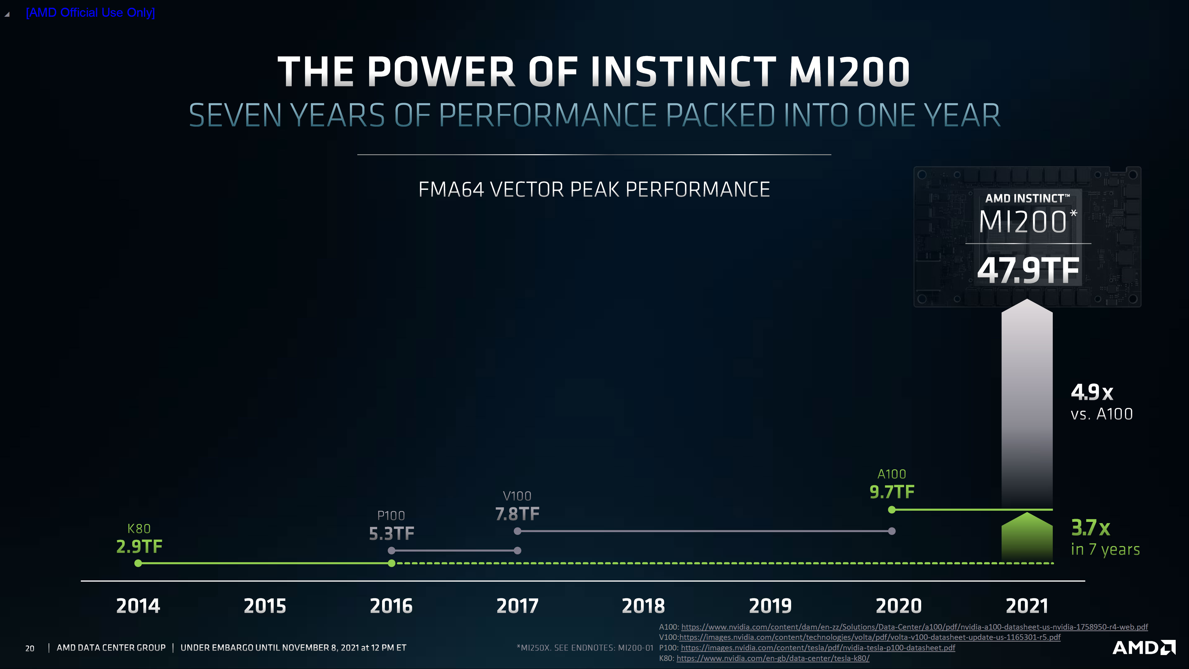
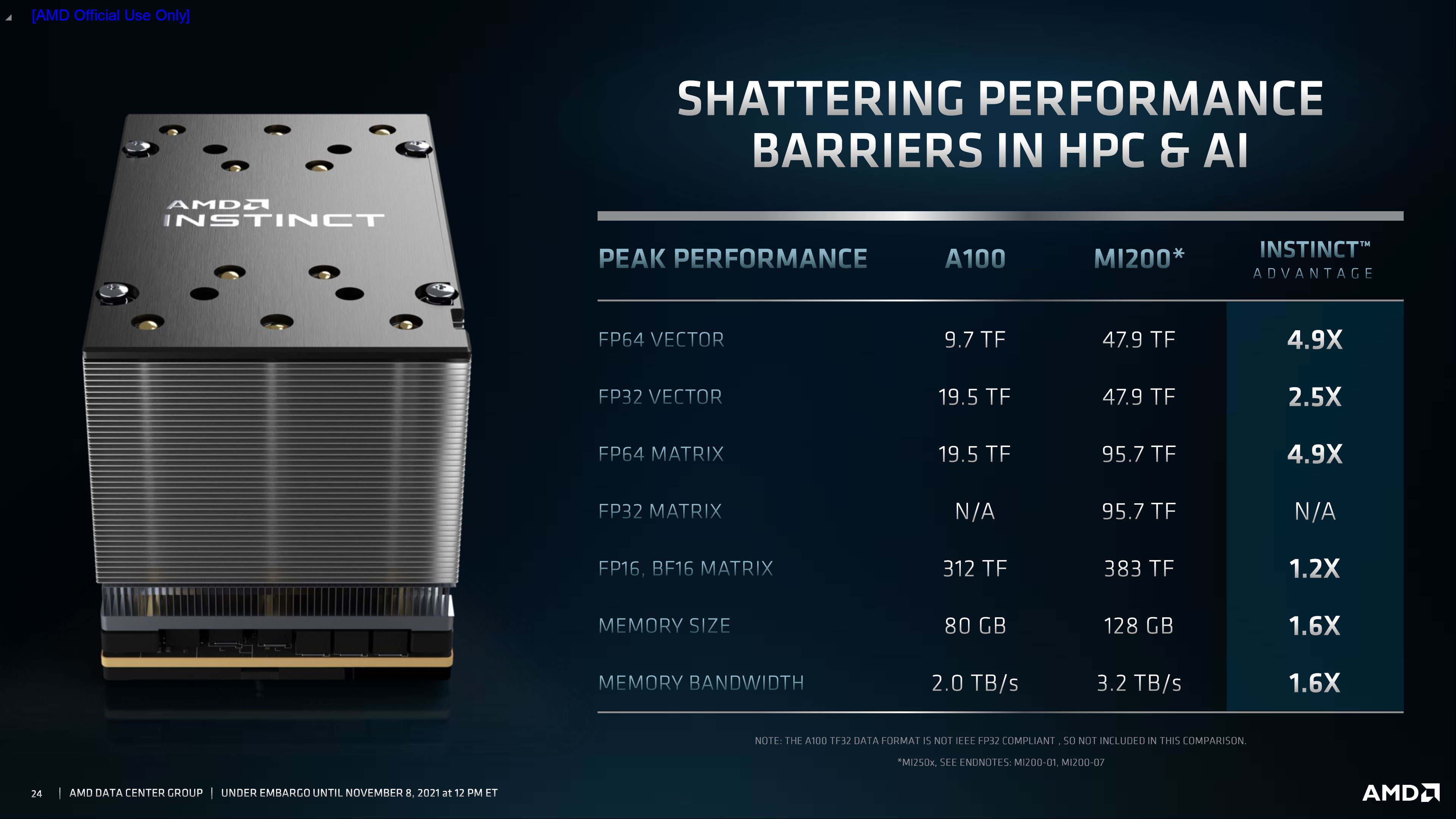
Putting that into numbers, MI100 was the first GPU to provide over 10 TFLOPS of FP64 vector compute. With its higher clocks, dual-GPUs, and doubled FP64 rates, the MI200 has a peak FP64 vector rate of 47.9 TFLOPS — AMD was quick to point out that this represents a 4.9X increase over the Nvidia A100 FP64 vector rates.
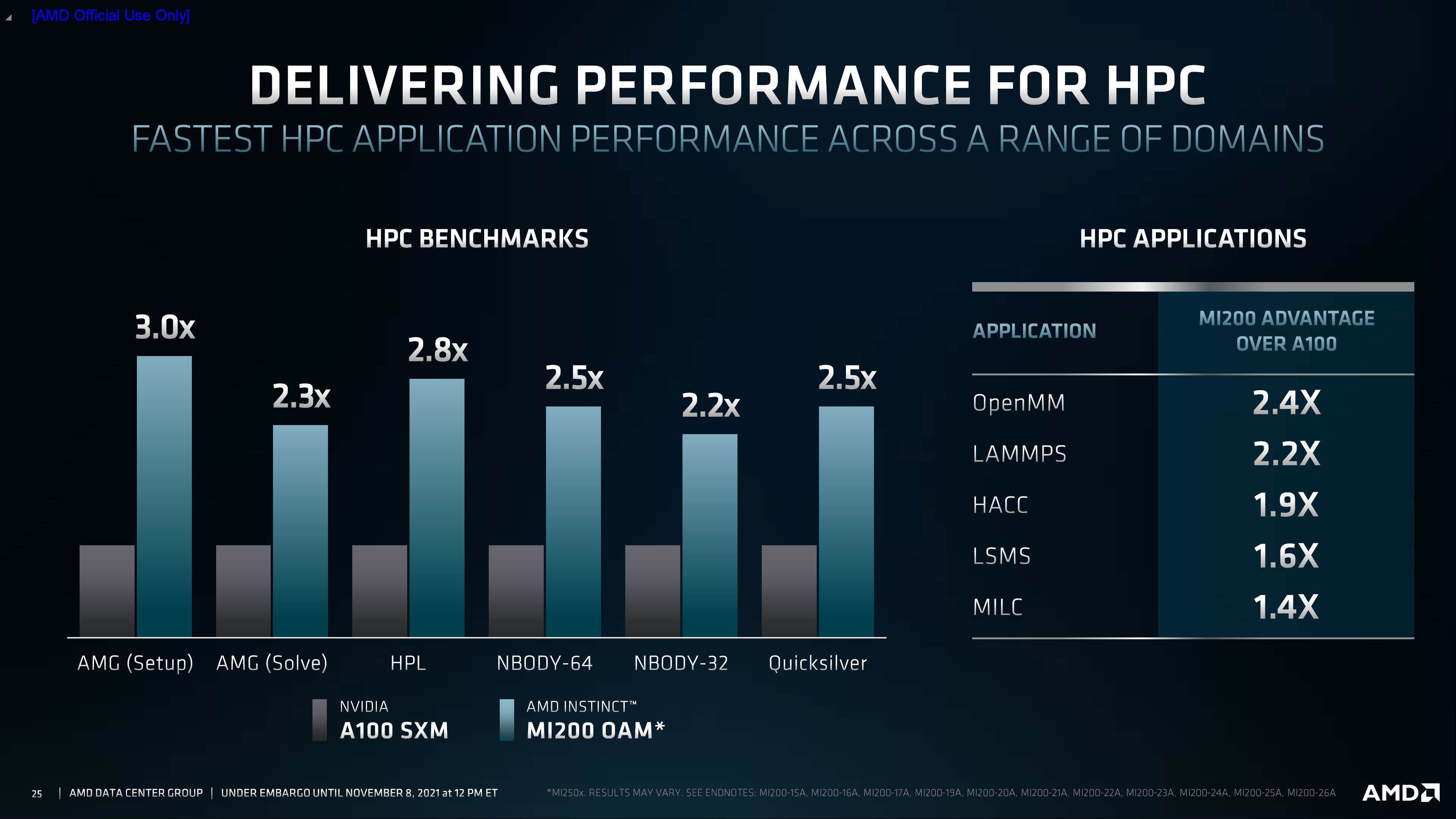
MI200 also adds FP64 matrix support, with a peak rate that's double the vector unit rate: 95.7 TFLOPS. Again, by way of comparison, the Nvidia A100 FP64 vector performance is 19.5 TFLOPS. That's on paper, of course, so we need to see how that translates into the real world. AMD claims performance is around three times as fast as the A100 in several workloads, though it's difficult to say if that will be the case across all workloads.
On the FP16 side of things, the performance isn't quite as high. Nvidia's A100 has 312 TFLOPS of FP16/BF16 compute, compared to 383 TFLOPS for the MI200, but Nvidia also has sparsity. Basically, sparsity allows the GPU to skip some operations, specifically multiplication by zero (which, so my math teacher taught me, is always zero). Sparsity can potentially double the compute performance of the A100, so there should be some use cases where Nvidia maintains the lead.
There are some key pieces of information that are still missing, like power requirements. The Nvidia A100 has a TDP of 400W for the SXM variant, which will be the direct competition for the MI200 OAM. Rumors are the MI250 OEM could have a TDP of up to 550W. For connectivity, Nvidia uses NVLink connections and AMD uses its Infinity Fabric, and we'll likely at least 6-way configurations of the MI200 OAM.
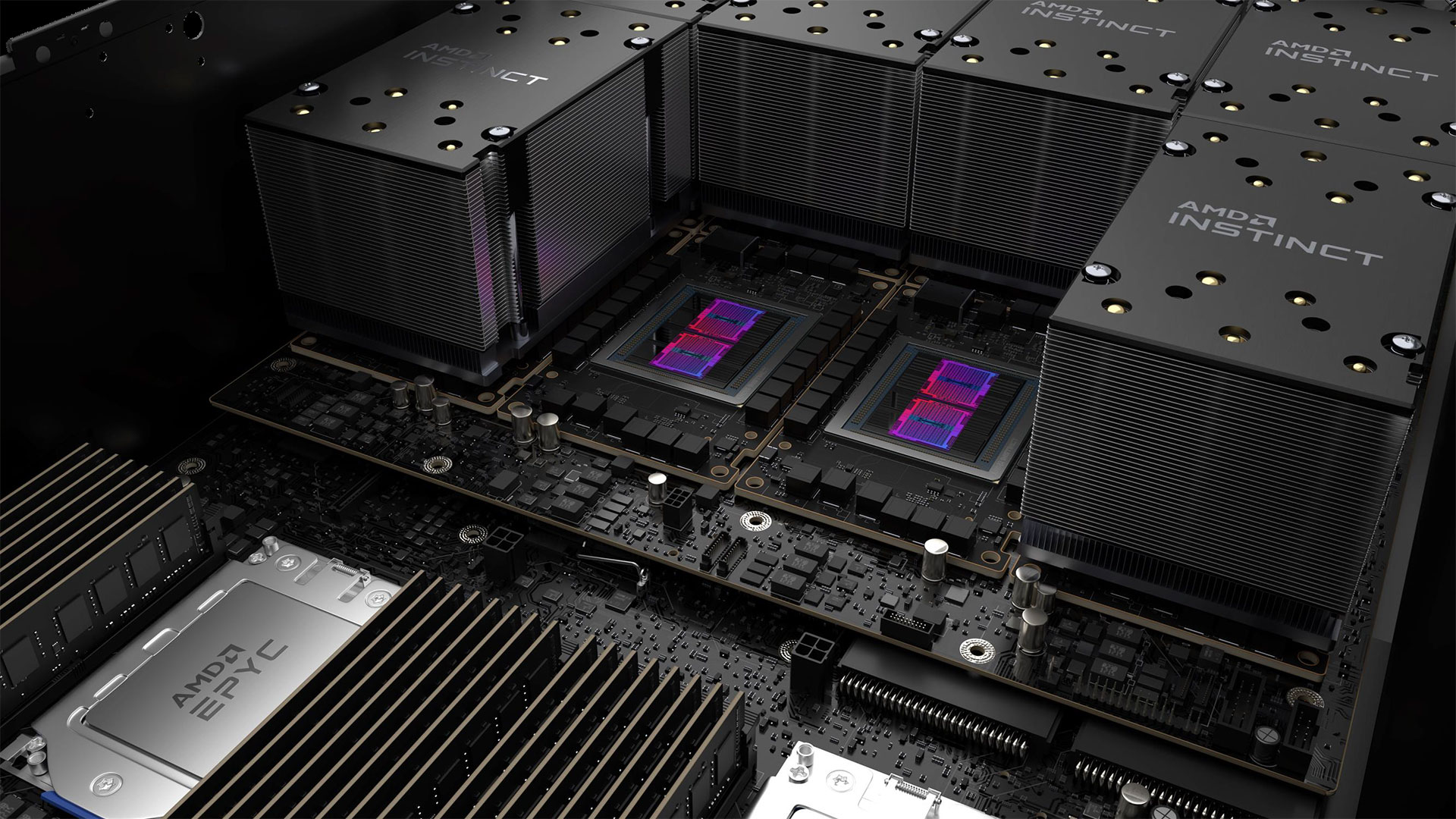
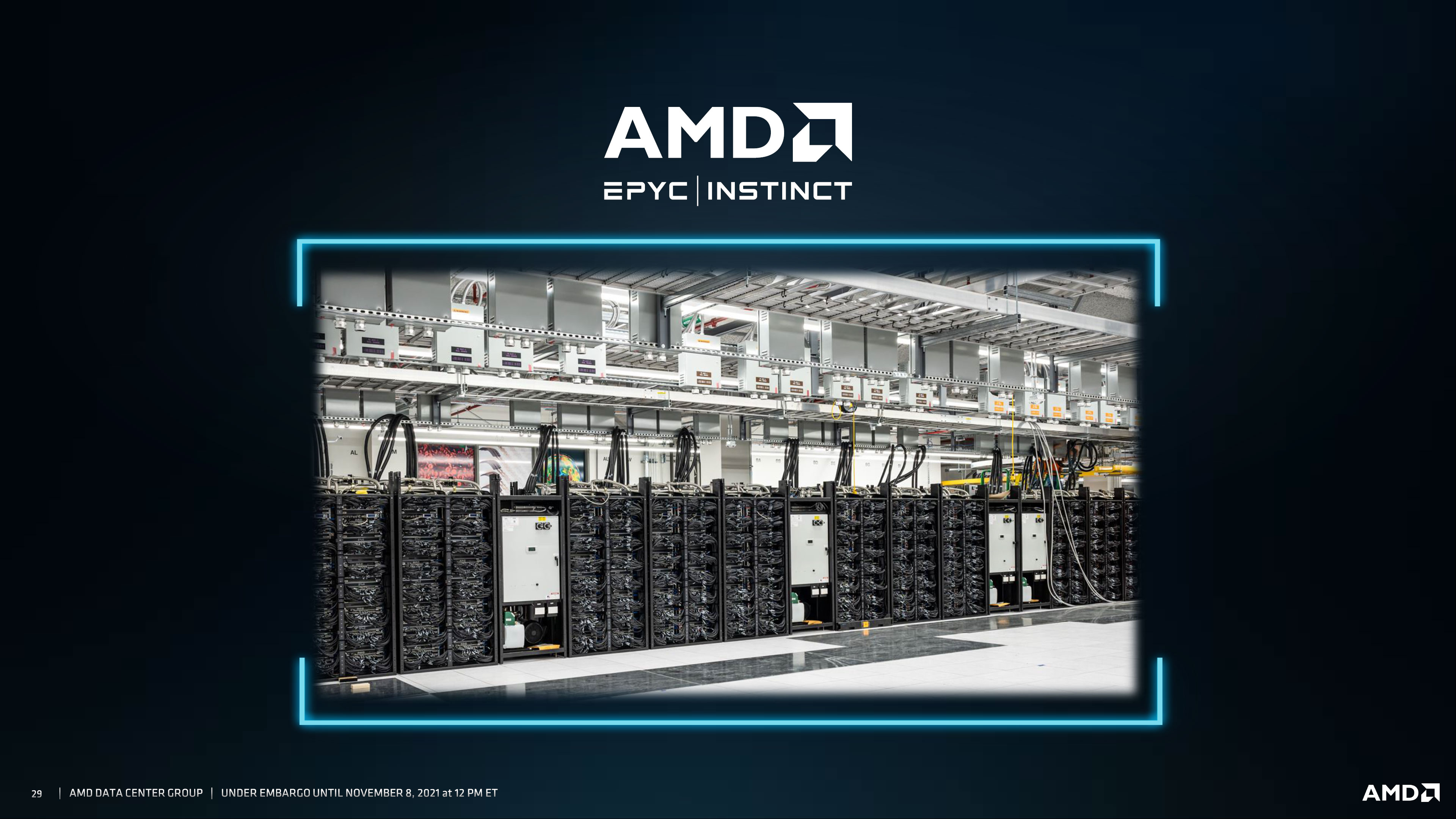
The above image comes from AMD's slide deck and presumably shows a rendering of a single node in the Oak Ridge National Labs Frontier supercomputer. Assuming it's an accurate picture, there will be six MI200 OAM GPUs paired with dual EPYC CPUs. ORNL's director Thomas Zacharia says that a single MI200 GPU provide more compute performance than an entire node in ORNL's previous Summit supercomputer. Frontier is currently being installed and will be available for researchers to begin using starting next year.
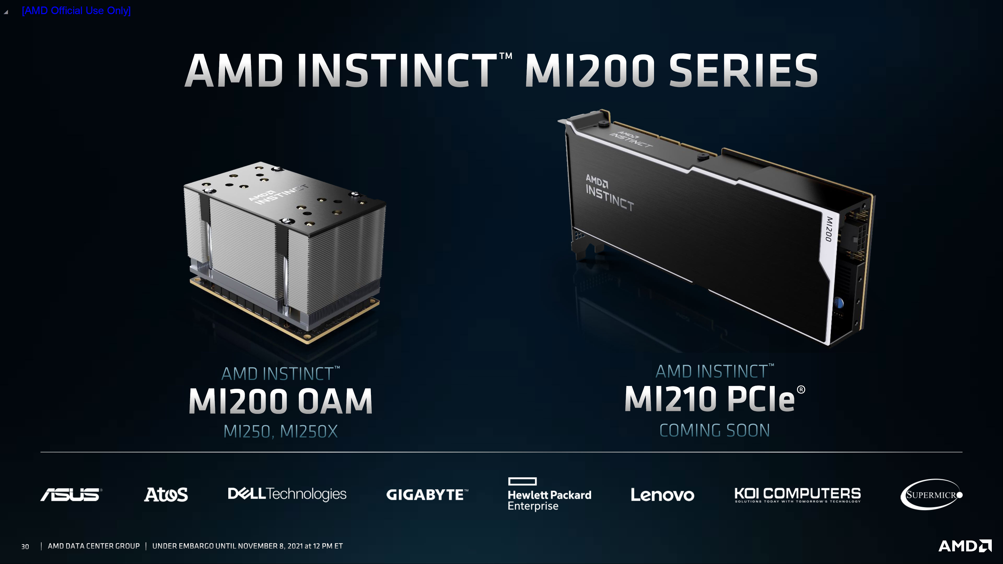
AMD has two models for the MI200 OAM currently planned. The higher performance MI250X, which we've used for most of this discussion, has 110 CUs per chiplet, while the lower MI250 drops down to 104 CUs per chiplet. That's the only real change, so the MI250 ends up with about 5% less compute performance. There will also be a PCIe version of the MI200 in the future.
There's plenty of other information to digest from AMD's accelerated data center premiere keynote, and we've covered the EPYC Genoa and Bergamo CPUs elsewhere. While Intel's Alder Lake CPUs may bring competition to AMD's existing consumer line, AMD's data center offerings still look incredibly potent.
The full slide deck of the MI200 section of the presentation is in the gallery below.




Get Tom's Hardware's best news and in-depth reviews, straight to your inbox.

Jarred Walton is a senior editor at Tom's Hardware focusing on everything GPU. He has been working as a tech journalist since 2004, writing for AnandTech, Maximum PC, and PC Gamer. From the first S3 Virge '3D decelerators' to today's GPUs, Jarred keeps up with all the latest graphics trends and is the one to ask about game performance.
