AMD Photonics Patent Reveals a Hybrid Future
Looking to accelerate scaling and power efficiency closer to the speed of light.
AMD has been secretly working on photonics technologies. While this is an expected development — photonics is one of the budding technological fields for both classical and quantum computing systems — it does represent a new venue for the company itself.
The information comes from a recently published patent, which AMD originally filed in the United States back in 2020. In this patent, the company describes a system that would allow for photonics-based communications systems to be directly connected to a chip.
Photonics takes advantage of the speed of light, which allows for much faster information transmission rates and increases energy efficiency (because there's no loss to electrical resistance from the usual mediums, such as copper). AMD's work in directly linking beams of light to a die would allow for improvements in latency and power consumption — which, in turn, would improve both performance and scalability.
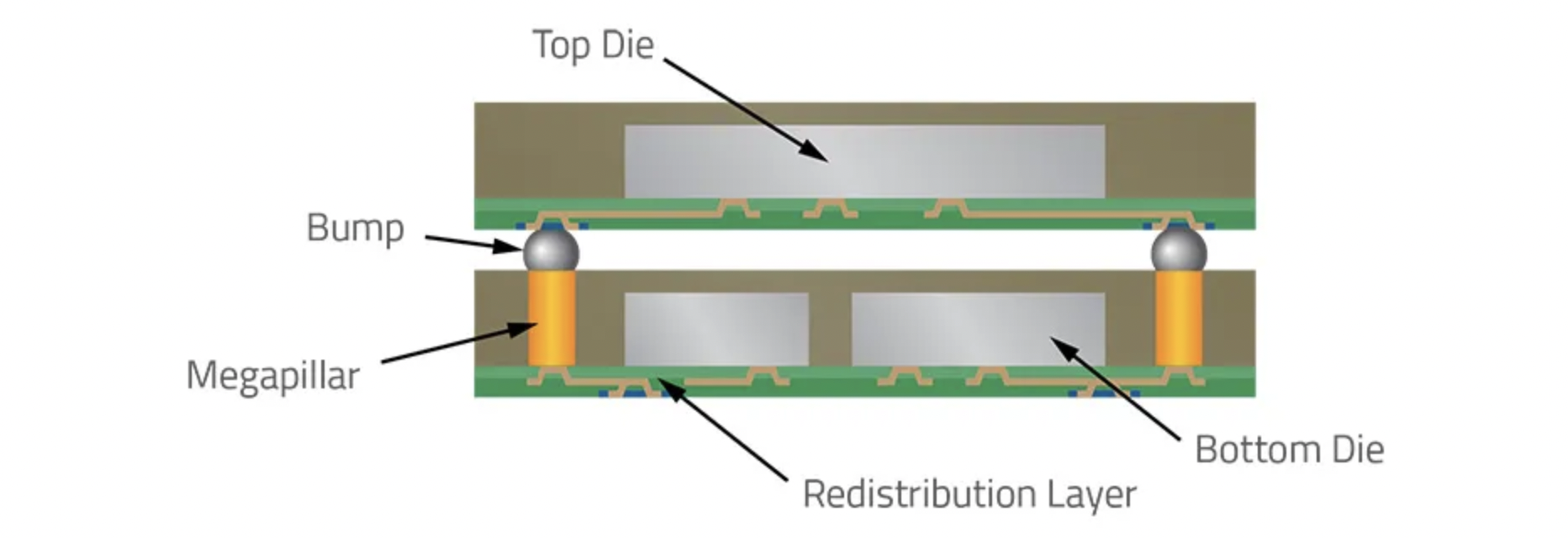
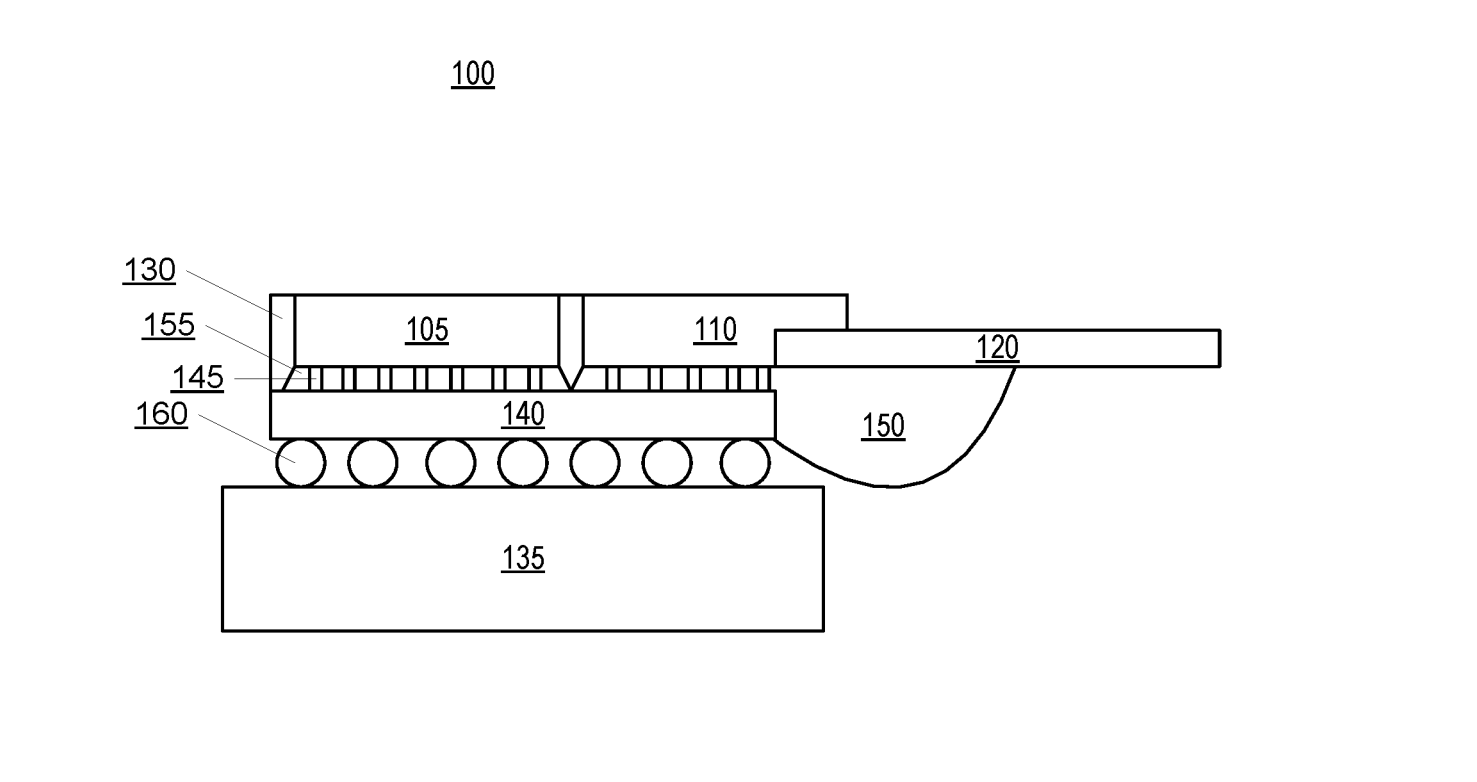
The patent — like most patents — is fuzzy. It generally describes the manufacturing steps needed to fabricate a chip that can handle photonic-based input and outputs. The manufacturing of such a chip would be necessarily different from those the company manufactures today, and would involve the integration of both a photonic and a silicon chip atop an organic redistribution layer (ORDL).

In current approaches, these layers lack the organic part (the O in RDL), and are usually metal-based interconnects that redistribute the I/O access to different parts of the chip — not unlike TSMC's Through-Silicon-Vias (TSV) technology that allows for 2D and 3D chip integration. So we're seeing an approach that's not unlike the usage of organic materials in OLED televisions and monitors, which in that case are used to emit light according to the electrical frequencies they're exposed to.

A typical SoC (System-on-Chip) is then added on top of this organic layer, enabling it to receive the redistributed light pulses that would ferry information in and out of the chip itself. The SoC computes information and passes it on to the photonic chip — placed alongside it — through the organic layer itself. This photonic chip would then transmit the information over a fiber optic cable to wherever it needs to go. And according to AMD's patent, these three components could all be manufactured on their own wafer substrates — facilitating the fabrication process — while being packaged together afterwards.
AMD's patent shows that the company is looking for ways to improve scalability that go beyond what conventional semiconductors allow. As the benefits from increasingly denser transistors have declined in recent years, while compute requirements have only gone up, chip designers have had to start looking for more creative ways to improve performance and — crucially — power efficiency.
Get Tom's Hardware's best news and in-depth reviews, straight to your inbox.
It's unlikely these technologies will make it into products anytime soon, let alone your next-door PC hardware store. But technology has a way of dropping lower in the cost scale. While initial hybrid applications of photonics and classical SoC may be a few years in the future, such venues of chip design are indispensable for further scaling in High Performance Computing (HPC) environments — where the big bucks are made.
The latter have also been hitting limits on air cooling capability for the increasingly denser, more energy-efficient, but ultimately more power-hungry, chips — and they, too, are looking for outside-the-box ideas to allow increased scaling — ideas such as liquid immersion cooling. Photonics' capability to transmit information without adding heat to these systems — while improving communications' speed and energy efficiency — sounds like a safe bet.

Francisco Pires is a freelance news writer for Tom's Hardware with a soft side for quantum computing.
-
jkflipflop98 Wow that's neat. I wonder which one of their factories they're going to use to make these?Reply
Oh wait. . . -
dipique Reply
Are you thinking that having an in-house traditional foundry would be a competitive advantage for photonics innovation? I don't see how.jkflipflop98 said:Wow that's neat. I wonder which one of their factories they're going to use to make these?
Oh wait. . .