BBCube 3D Memory Claimed to Offer 4x the Bandwidth of HBM2E
Researchers say this hybrid 3D memory could improve bandwidth between CPUs and GPUs.

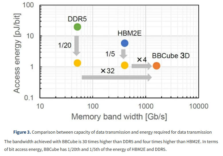
Tokyo Institute of Technology researchers have outlined their new BBCube hybrid 3D memory. BBCube 3D is short for 'Bumpless Build Cube 3D'. It is claimed that this new type of memory could pave the way to faster and more efficient computing by improving the bandwidth between processing units (or PUs, such as GPUs and CPUs) and memory chips. Specific claims for the technology are that it offers 30x bandwidth of DDR5 or 4X the bandwidth of HBM2E. Importantly, it also delivers impressive efficiencies by cutting bit access energy to one-twentieth of DDR5 memory, and a fifth of that used with HBM2E.
BBCube 3D's stacked architecture "has achieved the highest attainable performance in the whole world," boasts the official Tokyo Tech news blog. Before explaining how BBCube 3D memory is designed, the researchers outline the problem facing designers using currently available memory tech like DDR5 or HBM2E. They assert that desirable higher bandwidth currently comes at the expense of one or both of expensive wider buses, or power-intensive data rate boosts.

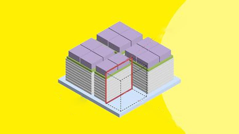
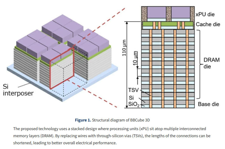
So, how does BBCube 3D improve the integration between PUs and dynamic random access memory (DRAM)? The diagram above gives a basic overview of the BBCube 3D design. You can see that the Pus sit atop their caches on top of the memory stacks. These are all housed on a silicon interposer foundation.
It is further explained that "the lack of typical solder microbumps, and the use of TSVs in place of longer wires, together contribute to low parasitic capacitance and low resistance." The structure creates connections between PUs and DRAMs in three dimensions, making extensive use of the aforementioned through-silicon vias (TSVs).

Tokyo Tech's claimed performance for BBCube 3D would make it highly attractive to computing designs thanks to a compelling combination of performance and reduced energy use. Another desirable quality of the design, stemming from the power efficiency, is said to be its reduced "thermal management and power supply issues," which can be precipitated by some 3D semiconductor designs.
There currently appear to be no plans in place for BBCube 3D commercialization, so let us join with the scientists at the Tokyo Institute of Technology in hoping that this new technology "paves the way to faster and more efficient computing."
Get Tom's Hardware's best news and in-depth reviews, straight to your inbox.

Mark Tyson is a news editor at Tom's Hardware. He enjoys covering the full breadth of PC tech; from business and semiconductor design to products approaching the edge of reason.
-
A similar concept was also worked on before, in 2022, although not same, but it was described as Bumpless Build Cube (BBCube) using Wafer-on-Wafer (WOW) and Chip-on-Wafer (COW) for Tera-Scale Three-Dimensional Integration (3DI).Reply
This was a quite interesting research paper though. Worth giving a read. Bumpless interconnect tech increased the number of TSVs per chip due to the finer TSV pitch and the lower impedance of bumpless TSV interconnects.
So when wafers with micrometer thickness were stacked, the total thickness was reduced, and the transistor capacity increased in proportion to the number of wafers.
Increasing the TSV interconnects density enabled terabyte-level bandwidth without sacrificing energy efficiency
https://www.mdpi.com/2079-9292/11/2/236 -
Kamen Rider Blade How the heck are you going to cool it?Reply
All those layers stacked, what about the heat that is near the centers and not near the edge of the structure? -
TechyIT223 Sounds interesting in theory but can they implement this without any complications? Heat should not be that much of an issue imoReply