Coffee Compound Makes Semiconductors More Productive, Too
Caffeic acid can improve current flow 100x, in some cases.

Researchers at the Advanced Industrial Science and Technology (AIST) institute in Japan say the use of a coffee compound can increase current flow in semiconductor components by up to 100x. Specifically, a thin layer of caffeic acid on the surface of an electrode facilitated a vastly improved current flow through an organic semiconductor device, according to their work.
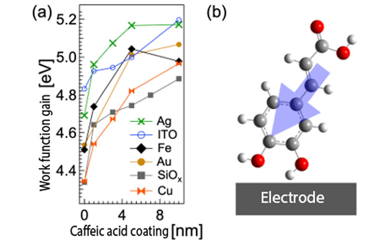
The science behind this remarkable improvement in current flow is explained by the AIST blog. A report on the research carried out at the Tsukuba facility says that the action of the caffeic acid on the electrode causes molecules on the surface of the component to spontaneously line up, reducing the resistance to current flow. Hence the 100x boost to current flow.
This discovery is going to be useful in the development of future organic semiconductor devices, such as organic light-emitting diodes (OLEDs) and organic solar cells (OPVs), say the scientists. It is claimed the discovery will be particularly valuable in promoting sustainability. Thanks to the application of a thin caffeic acid layer, derived from plants, the use of environmentally unfriendly or unsustainable chemical resources can be lessened or avoided.
Article continues belowCurrently, manufacturers of organic semiconductors use materials with problematic qualities for the environment in the role of the electrode modification layer. One choice for this layer, a polymer called Pedot:PSS, raises concerns about environmental pollution. An alternative, a Molybdenum trioxide material, uses an oxide of a scarce metallic element.

AIST researchers conducted tests using caffeic acid and a variety of electrode materials, including gold, silver, copper, iron, indium tin oxide (ITO), and silicon with a native oxide layer. You can see in the chart that the electrode work function increased by as much as 0.5 eV after the caffeic acid treatment. Note that the researchers say the thin film of caffeic acid does not dissolve in the organic solvents used in the production of organic semiconductor thin films, so it's eminently suitable for this purpose.
So far so good, but what next? The researchers at AIST hope to apply this electrode modification / coating technology in organic semiconductor devices like the aforementioned OLEDs and OPVs, with the eventual goal that semiconductor components and IoT devices be fabricated entirely by sustainable means, as well as being easy to recycle.
Get Tom's Hardware's best news and in-depth reviews, straight to your inbox.

Mark Tyson is a news editor at Tom's Hardware. He enjoys covering the full breadth of PC tech; from business and semiconductor design to products approaching the edge of reason.
-
Co BIY Interesting although I don't think semi-conductors are in danger of using to much of the 68,000 tons of molybdenum mined in the US each year (not even the world leader in production).Reply