Huawei Turns To 3D Chip Stacking, Could Potentially Circumvent US Sanctions
Huawei plans to boost performance for chips based on older nodes.
Huawei has developed (and patented) a chip stacking process that promises to be significantly less expensive than existing chip stacking methods. The tech will help Huawei continue to develop faster chips using older mature process tech, which could theoretically help it avoid US sanctions.
The only question is whether Huawei can actually take advantage of its innovation, given that foundries cannot produce chips for the company without an export license from the U.S. government. But at least Huawei itself certainly believes that it can, especially given that this tech could provide a performance boost for chips based on older nodes that aren't subject to such harsh US restrictions.
A Way to Stay Competitive
We'll get to the details of the new tech below, but it's important to understand why Huawei is developing this new tech. Since the U.S. government blacklisted Huawei and its chip design subsidiary HiSilicon and now requires all companies making silicon for them to apply for an export license since all semiconductor production involves technologies developed in the U.S., Huawei can't access any modern node (e.g., TSMC's N5), and therefore has to rely on mature process technologies.
Article continues belowTo that end, innovative chip packaging and chiplet interconnection technologies in general as well as 3D stacking in particular is a way for the company to throw in more transistors into its SoCs and get the performance it needs to be competitive, said Guo Ping, Huawei's former rotating chairman, at a recent news conference, reports DigiTimes. Therefore, it makes great sense for the company to invest in proprietary packaging and interconnection methods, such as the one it patented.
"Micro-nano technology, exemplified by 3D hybrid bonding technology, will be the primary means to extend Moore's Law," said Guo.
The high-ranking executive from Huawei indicated that since modern leading-edge process technologies are progressing relatively slowly, multi-chiplet designs in 2.5D or 3D packages are a general way for chip designers to keep throwing more transistors into their products and meeting the expectations of their clients in terms of new features and performance. Therefore, Huawei will continue to invest in area enhancing and stacking technologies for in-house designs, the former chairman stressed.
The claim made publicly at a news conference clearly indicates that Huawei aims to use its hybrid TSV-free 3D stacking method (or maybe a similar and more mainstream method) for its upcoming products. The main question is whether the method requires any tools or technologies that the U.S. government may deem cutting-edge and not grant an export license (after all, most of the fab tools use technologies that originated in the USA). That said, whether we'll see a foundry making 3D chiplet packages for Huawei using the latter's patented method remains to be seen. But at least Huawei has a unique technology for inexpensive 3D stacking that can help it to stay competitive even without access to the latest nodes.
Get Tom's Hardware's best news and in-depth reviews, straight to your inbox.
Stacking Without Vias
Innovative chip packaging and multi-chiplet interconnection technologies are set to become crucial in the next few years for leading-edge processors, and so all major chip developers and manufacturers now have their own proprietary chip packaging and interconnection methods.
Chipmakers generally use two packaging and interconnection methods: 2.5D packaging that enables a high-density/high-bandwidth in-package interconnect for chiplets sitting next to each other, and 3D packaging that makes processors smaller by stacking different chiplets on top of each other. However, 3D packaging typically requires rather complex wiring since chiplets need to communicate and power has to be delivered using TSVs.
While TSVs have been used in chip manufacturing for over a decade, they add complications and costs to the packaging process, so Huawei decided to invent an alternative solution without TSVs. What Huawei's specialists designed is essentially a hybrid between 2.5D and 3D stacking, as two chiplets overlap each other inside the package, saving space, but do not exactly sit on top of each other like in classic 3D packages.
3D Stacking with Overlapping
Huawei's method uses overlapping parts of the chiplets to establish a logical interconnection. Meanwhile, two or more chiplets still have their own power delivery pins connected to their own redistribution layer (RDL) using a variety of methods. But while Huawei's patented technology avoids using TSVs, it does not look easy and cheap to implement.
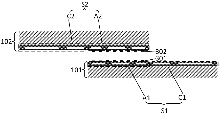
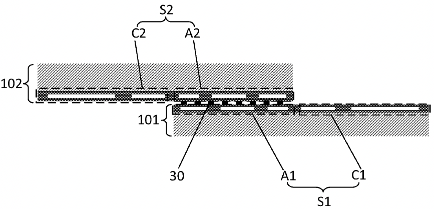
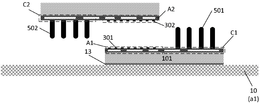
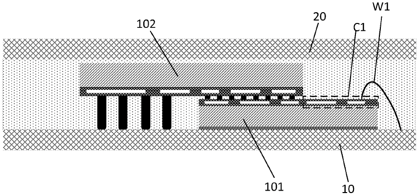
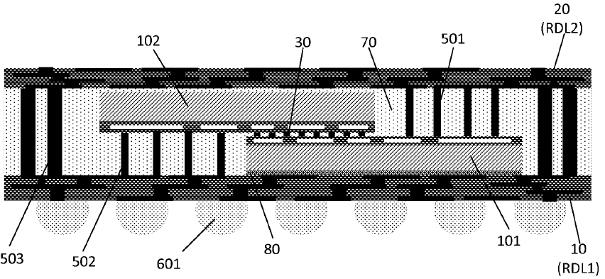
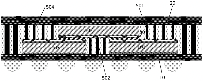
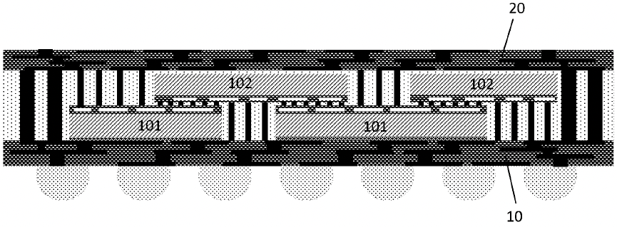
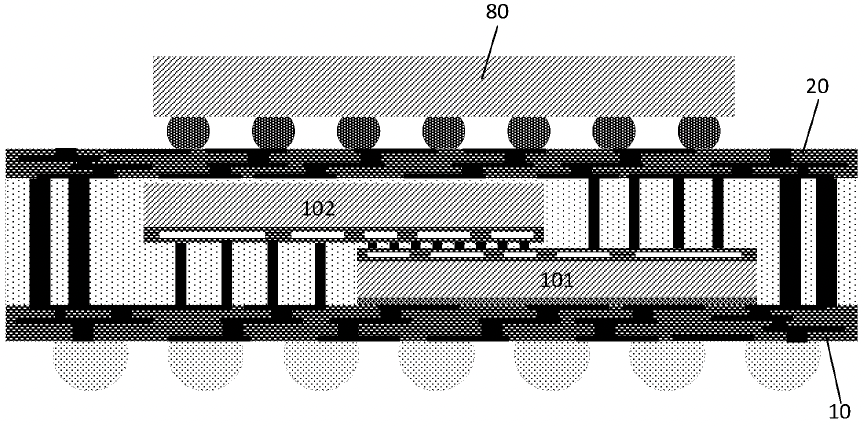
Huawei's process involves flipping one of the chiplets upside down before connecting to another (or others). It also requires building at least two redistribution layers to deliver power (e.g., two chiplets means two RDLs, three chiplets can still use two RDLs, so do four, see the above gallery for details), which is not particularly cheap as it adds several additional process steps. The good news is that the redistribution layer of one of the chips can be used to connect things like memory, thus saving space.
In fact, Huawei's hybrid 3D stacking method may arguably be more universal than other companies' traditional 2.5D and 3D packaging technologies. For example, it is rather hard to stack two or three power-hungry and hot logic dies on top of each other, as cooling such a stack will be very complicated (which may ultimately mean compromises with clocks and performance). Huawei's method increases the surface size of the stack, which simplifies cooling. Meanwhile, the stack is still smaller than a 2.5D package, which is important for mobile applications like smartphones, notebooks, or tablets.
Not Alone
It is noteworthy that Semiconductor Manufacturing International Corp. (SMIC) with whom Huawei reportedly plans to build a fab, is also betting on advanced packaging and interconnection technologies as on a way to get around sanctions imposed by the U.S. government. The company cannot get access to manufacturing tools required to make chips using sub-10nm fabrication technologies, so advanced packaging and interconnection methods are crucial for SMIC as well.
Other contract makers of semiconductors (TSMC, GlobalFoundries), integrated design manufacturers (Intel, Samsung), and even fabless chip developers (AMD) that can get access to leading-edge fab tools and process technologies also develop their own 2.5D and 3D chiplet stacking and interconnection methods to offer their clients or for their future products. Thus, Huawei is just following the curve.

Anton Shilov is a contributing writer at Tom’s Hardware. Over the past couple of decades, he has covered everything from CPUs and GPUs to supercomputers and from modern process technologies and latest fab tools to high-tech industry trends.
-
jkflipflop98 The author of this article is mistaken. F2F (face to face) stacking methods are nothing new. Their problem is they have incredible heat buildup as all the thermals are contained inside of a tiny strip that's sandwiched in between the silicon substrates of the die. It acts like a blanket keeping the heat inside. Terrible for thermals and that's why no one else does this.Reply -
KananX It’d strange if they could circumvent the export restrictions with this, but if yes, kudos to them for their creativity. The export restrictions don’t make much sense anyway.Reply -
Kamen Rider Blade Good luck with cooling that sucker.Reply
You have Heat trapped in the center and heat on both sides of the chips.
That's going to be a unnecessarily complex die to cool. -
KananX Reply
Probably just a flagship chip but who knows.Kamen Rider Blade said:Good luck with cooling that sucker.
You have Heat trapped in the center and heat on both sides of the chips.
That's going to be a unnecessarily complex die to cool.
