10nm Ice Lake CPU Meets M.2: The 'Spring Hill' Nervana NNP-I Deep Dive
Intel revealed the broad outlines of its new Nervana Neural Network Processor for Inference, of NNP-I for short, that comes as a modified 10nm Ice Lake processor that will ride on a PCB that slots into an M.2 port (yes, an M.2 port that is normally used for storage), at an event in Haifa, Israel two months ago. Today, the company provided further deep-dive details of the design here at Hot Chips 31, the premier venue for leading semiconductor vendors to detail their latest microarchitectures.
Intel is working on several different initiatives to increase its presence in the booming AI market with its 'AI everywhere' strategy. The company's broad approach includes GPUs, FPGAs, and custom ASICs to all tackle different challenges in the AI space, with some solutions designed for compute-intensive training tasks that create complex neural networks for object recognition, speech translation, and voice synthesis workloads, to name a few, and separate solutions for running the resulting trained models as lightweight code in a process called inference.
Intel's Spring Hill Nervana Neural Network Processor for inference (NNP-I) 1000, which we'll refer to as the NNP-I, tackles those lightweight inference workloads in the data center. The chips are small enough to be mounted on a standard M.2 device, which then slots into a standard M.2 port on a motherboard, to offload Xeon servers from inference-intensive workloads, thus freeing the bigger chip up for general compute tasks. As we covered recently, the Neural Network Processor for Training (NPP-T) slots in as Intel's Nervana solution for training workloads, but the two devices have vastly different underlying architectures.
Spring Hill NPP-I
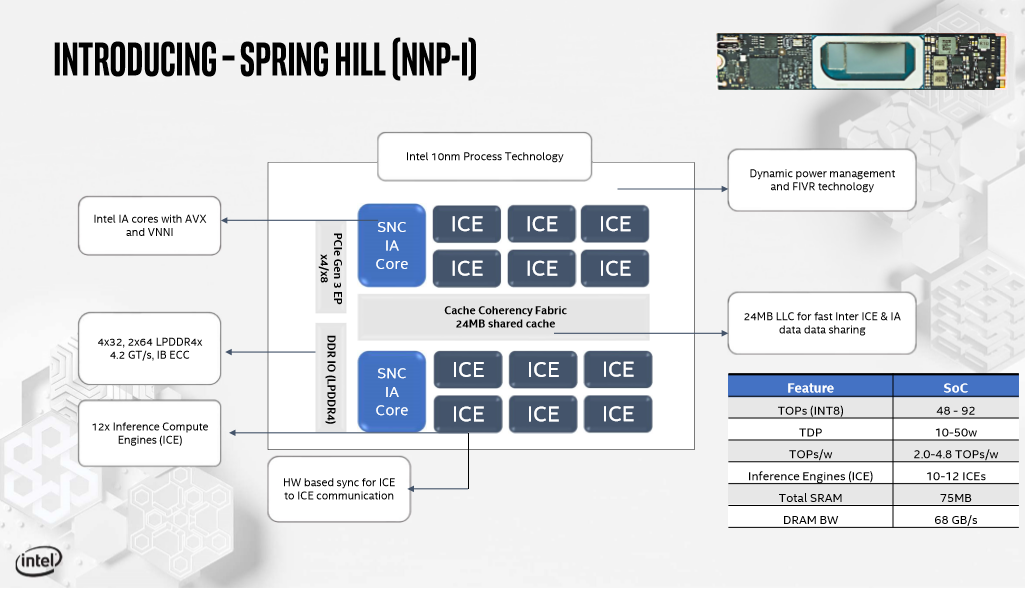
Intel modified the 10nm Ice Lake die, removing two compute cores and the graphics engine to accommodate 12 Inference Compute Engines (ICE). The ICE accelerators, which have hardware-based synchronization between units, share a coherent fabric and 24MB of L3 cache with the two IA cores that have the Sunny Cove microarchitecture.
The IA cores are standard Ice Lake cores that support AVX-512 and VNNI instructions that speed up convolutional neural networks, while a fully-integrated voltage regulator (FIVR) delivers power to the components dynamically to allocate more of the power budget to the most active on-die units. The die comes with two LPDDR4X memory controllers that connect to the on-package memory, which you can see as a single component on the lower left of the M.2 PCB. The controllers provide up to 4.2 GT/s (68 GB/s) of throughput and support in-band ECC.
Intel isn't sharing LPDDR4 capacity, or other fine-grained details about the M.2 device yet. We do know that Intel mounts the package on different forms of add-in cards, like the M.2 version pictured above, which can then slip into the standard M.2 port on a server motherboard, or on larger add-in cards that slot into a standard PCIe slot. Unlike some custom silicon designed for AI, like Google’s TPU, this device is broadly hardware-compatible with almost all existing modern servers. The approach is also scalable: You can add as many NNP-I’s to the server as needed, especially with PCIe risers that house multiple M.2 ports.
The device communicates across either a PCIe 3.0 x4 or x8 interface with the host, but it doesn't use the NVMe protocol. Instead, it operates as a standard PCIe device. Intel will provide software that orchestrates moving inference ‘jobs’ to the accelerator entirely, which will then notify the Xeon CPU when the work is done. The offloading eliminates the Xeon’s back-and-forth communication across the PCIe bus with other types of accelerators, which is taxing for the CPU because it generates interrupts and requires data movement. In contrast, the NNP-I works as a self-contained system with its own I/O accommodations (PCH) that allow it to access the data required for processing.
Get Tom's Hardware's best news and in-depth reviews, straight to your inbox.
The device can support different power envelopes that range from 10W to 50W, which has an impact on performance. The M.2 interface’s 15W limitation hinders power delivery to devices plugged into a standard M.2 socket, but NNP-I’s in larger add-in cards can operate at the highest TDP ratings, meaning they offer much more performance. TOP/s range from 48 to 92 with INT8 operations. Depending on the configured TDP, the die provides efficiency of 2 to 4.8 TOP/s per watt, but that metric doesn't include total package power.
Inside The Inference Compute Engine
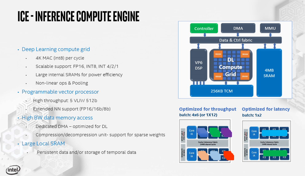
Diving into the ICE engines reveals that each of the ICE units has an additional 4MB of SRAM to help reduce intra-die data movement, which is always more expensive in terms of power and time than the actual compute operations. The Deep Learning Compute Grid is a tensor engine that is connected via a data and control fabric to the SRAM and a VP6 DSP. The DSP engine can be used for algorithms that aren’t specifically tuned for the fixed-function DL Compute Grid. Also, other code can run with VNNI on the Ice Lake cores, enabling multiple models to run on the device simultaneously and also providing a bit of needed forward-compatibility for the fast-moving AI space.
The DL Compute Grid accommodates FP16 and INT8 but is also designed to support INT4, 2, and 1 to support possible future adjustments to AI algorithms. Surprisingly, it doesn't support bfloat16. The fabric can be optimized either for bandwidth or latency, as shown in the bottom right tables, by adjusting how workloads are spread among the ICE units.
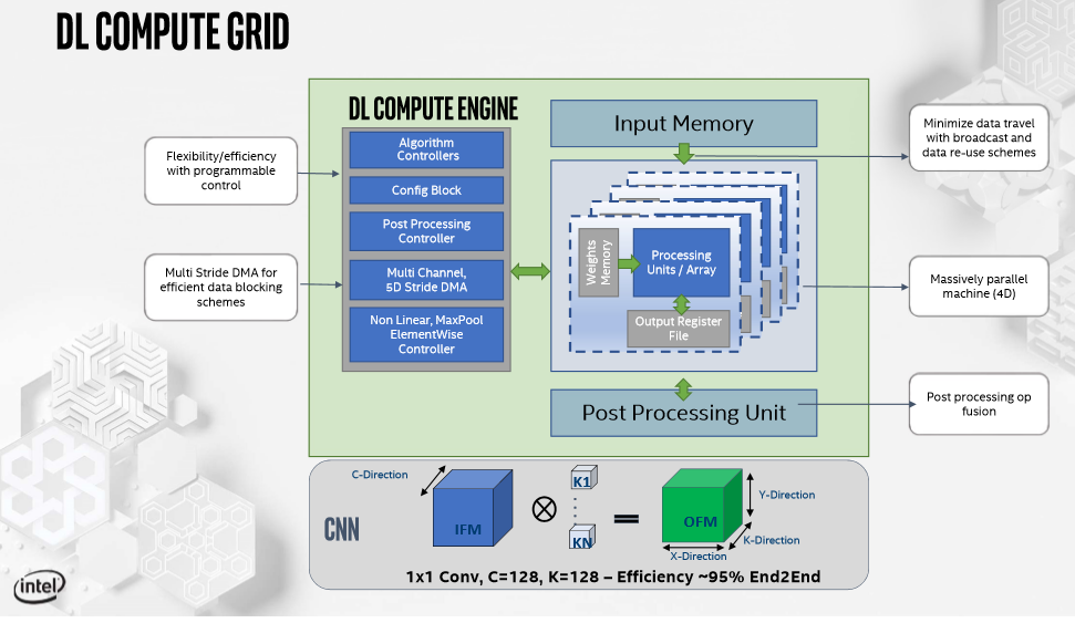
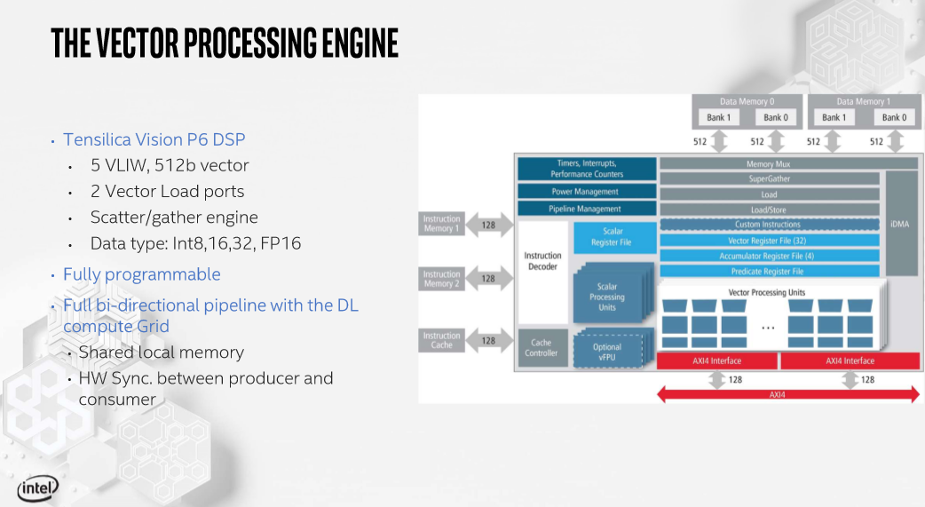
Here we can see the close-up views of the DL Compute Grid, which is designed to be flexible to maximize its 4D parallel compute capabilities, and the Tensilica Vision P6 DSP that's used for vector processing. The Tensilica DSP engine is a wide VLIW machine that supports INT8, 16, 32, and FP16. The engine is fully programmable and features a bi-directional pipeline with the DL Compute Grid to transfer data quickly between the two hardware-synchronized units.
Spring Hill Memory Subsystem
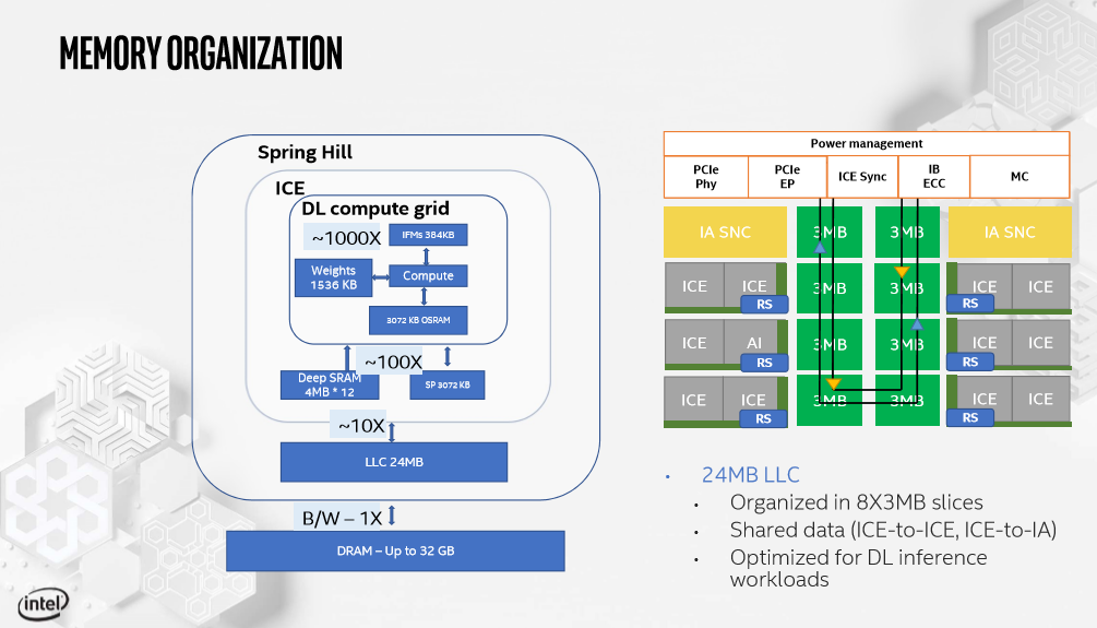
Zooming back out to the memory subsystem reveals many of the rationalizations behind the design decisions made in each of the compute units. Here we can see that the hardware-controlled L3 cache is broken up into eight 3MB slices shared among the AI cores and ICE units. The design is optimized to keep data as close to the compute engines as possible with four distinct layers.
The series of blocks on the left of the chart quantify the latency hit for moving data through each layer of the memory hierarchy. With a data transfer from DRAM to the DL Compute Grid set as the baseline, we can see how much faster each layer of the hierarchy can deliver data to the engine. An access from L3 cache is 10X faster than DRAM, while data stored in the DL Compute Grid is 1000X faster.
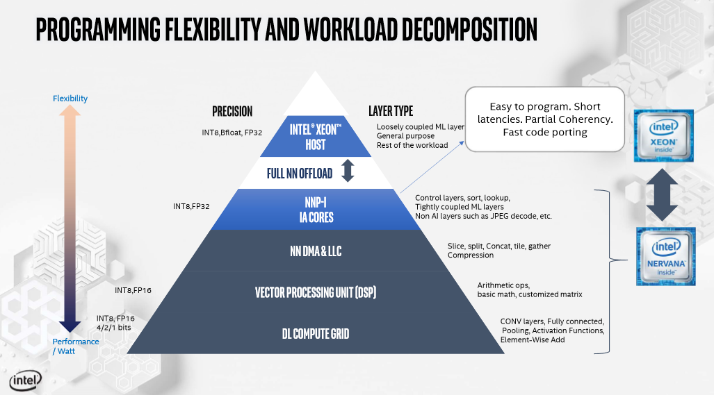
In summary, the tiered design allows the Xeon to offload several different types of neural networks to the device, and each layer supports certain levels of precision. You'll also notice that the pyramid above is aligned based on performance-per-watt.
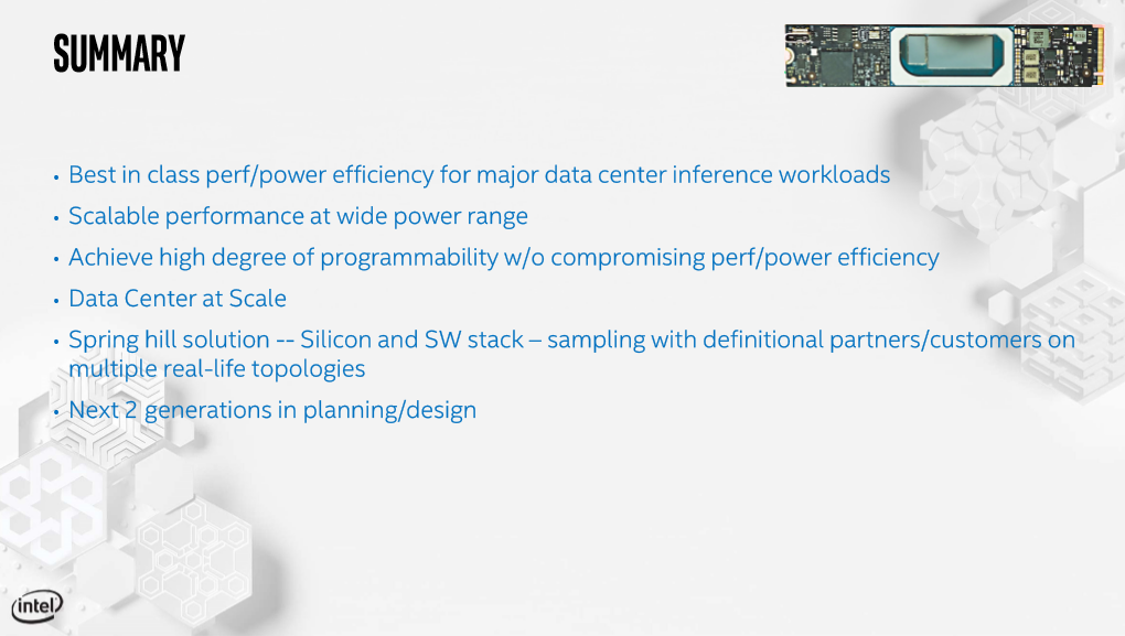
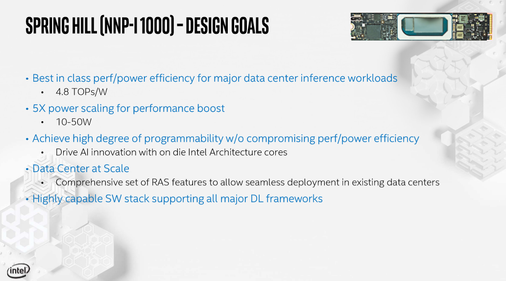
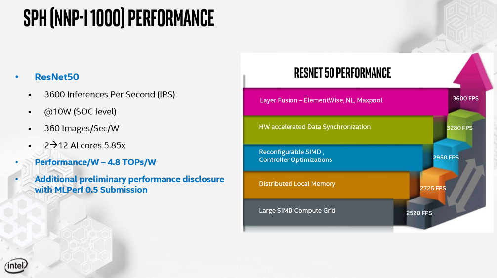
Intel shared performance data with ResNet50 running at 3,600 inferences per second with the chip set at a 10W TDP. That equates to a 4.8 TOP/s-per-watt efficiency measurement, which meets the company's design goals. Notably, the chip is more efficient at lower TDP ranges, so efficiency could vary at higher-performance settings. These numbers also only apply to the ASIC and do not include the power draw of the full M.2 device. Intel says it will share more performance data in the future.
Intel provides a compiler that tailors code to the NNP-I’s accelerators and is working with Facebook, which served as the company’s “definitional’ partner during development, to ensure the Glo compiler also supports the device. The device also supports all standard languages, like PyTorch and TensorFlow, among many others, with little to no alteration. Intel maintains that anyone who can work with Xeons for inference can use the NNP-I, but that ninja programmers can get in the weeds to deeply optimize for the tiered architecture.
Inference applications are far more prevalent than training in the data center, and affordable power-efficient devices will sell en masse to hyperscalers and cloud service providers (CSP), meaning this could become a lucrative segment for Intel. The firm doesn’t envisage these devices coming to retail, per se, but the company does expect CSPs to expose them via cloud-based instances in the future.
Intel already has two more generations of the NNP-I in development. The company will kick off volume production by the end of the year, and NNP-I's are already sampling.

Paul Alcorn is the Editor-in-Chief for Tom's Hardware US. He also writes news and reviews on CPUs, storage, and enterprise hardware.
-
Geef So we are looking at the high end version of a Math Co-Processor.Reply
Runs back to my old 486 SX 33. "I knew saving you was for the good of us all!" -
thegriff Reply
Yep, sounds like it, but just for a different purpose. Everything comes around just like we all used mainframes etc with terminals on our desks to stand alone computers now back to basically mainframes in a sense with the cloud. Lifes just one big circle. :)Geef said:So we are looking at the high end version of a Math Co-Processor.
Runs back to my old 486 SX 33. "I knew saving you was for the good of us all!" -
GetSmart Reply
The old 80486SX models do not have a math co-processor. Only the 80486DX models have them.Geef said:So we are looking at the high end version of a Math Co-Processor.
Runs back to my old 486 SX 33. "I knew saving you was for the good of us all!" -
JayNor So, looks like the intent is that the processing is done by the Cadence Tensilica V6 DSPs , one per ICE. The two sunny cove processors add two avx512 units, including dlboost, but also fp32 operations, which wouldn't be the primary processing.Reply
I noticed the Hololens 2 also uses these DSPs
You can get clear pdfs of the slides through the intel newsroom announcement.
https://newsroom.intel.com/news/hot-chips-2019/ -
Geef ReplyGetSmart said:The old 80486SX models do not have a math co-processor. Only the 80486DX models have them.
Sorry I didn't reply to this sooner. I know the SX version didn't have a math co-processor. I remember the choice and the price difference when I got my machine back then. I didn't need the extra power so I went cheap. Oh yeah I could run DOS 6.2 with Windows 3.1 great on that baby. -
GetSmart Reply
And if the motherboard features a socketed CPU then can upgrade to 80486DX or 80486DX2. The math co-processor can often have significant performance difference in 3D games and some software. However if the motherboard features a soldered QFP CPU then no upgrade path. Also sometimes those motherboards have a socket for the math co-processor, but getting one of those math co-processors is rather difficult.Geef said:Sorry I didn't reply to this sooner. I know the SX version didn't have a math co-processor. I remember the choice and the price difference when I got my machine back then. I didn't need the extra power so I went cheap. Oh yeah I could run DOS 6.2 with Windows 3.1 great on that baby. -
JayNor ReplyJayNor said:So, looks like the intent is that the processing is done by the Cadence Tensilica V6 DSPs , one per ICE.
To reply to my own comment ... after reading more, it looks like those Tensilica DSPs have a minor role relative to the processing that occurs in those big multiplier arrays.

