Intel Deep Dives on Nervana NNP-T: 27 Billion Transistors, 32GB of HBM2 Packed on 688mm-Squared Die
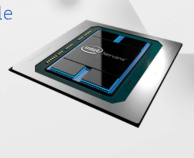
Intel revealed fine-grained details about its much-anticipated Spring Crest Deep Learning Accelerators here at Hot Chips 31. The Nervana Neural Network Processor for Training (NNP-T) comes with 24 processing cores and a new take on data movement that's powered by 32GB of HBM2 memory. The spacious 27 billion transistors are spread across a 688mm2 die. Oddly enough, the NNP-T also incorporates leading-edge technology from Intel-rival TSMC.
Artificial intelligence and machine learning have taken the data center by storm, redefining how compute is used and deployed at scale in an exceedingly short period of time. As such, the rise of GPUs, long the go-to solution for AI training workloads, in the supercomputing space has been explosive. In 2008, not one supercomputer used a GPU for computation, instead relying on the tried-and-true CPU, but now 80 percent of compute power in the top 500 supercomputers comes from GPUs. As we've seen time and again, the trends in HPC and supercomputing filter down to the broader data center, so the proliferation of AI/ML workloads presents a threat to Intel's data center dominance, as each GPU replaces several Xeon processors.
In response, Intel has developed a multi-pronged approach to keep its hands on the steering wheel. Compute-heavy training workloads create complex neural networks that run object recognition, speech translation, and voice synthesis workloads, to name a few, which are then deployed as lightweight inference code. Due to their ubiquity, Xeon processors continue to be the platform of choice for the less computationally-intense inference workloads, but Intel is developing several solutions to tackle the training workloads that firmly remain the stomping grounds of Nvidia's GPUs.
Nvidia claims that GPUs are the end-all-be-all solution for all forms of AI and machine learning, but Intel maintains that there are different solutions for each class of workload. Part of Intel's answer to training will come in the form of its forthcoming Xe Graphics Architecture and Altera-derived FPGAs, but the company also has a new line of custom-built Nervana silicon in the works for training workloads.
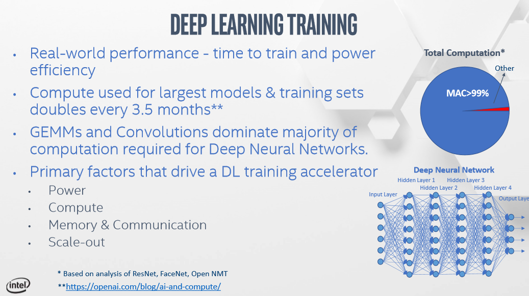
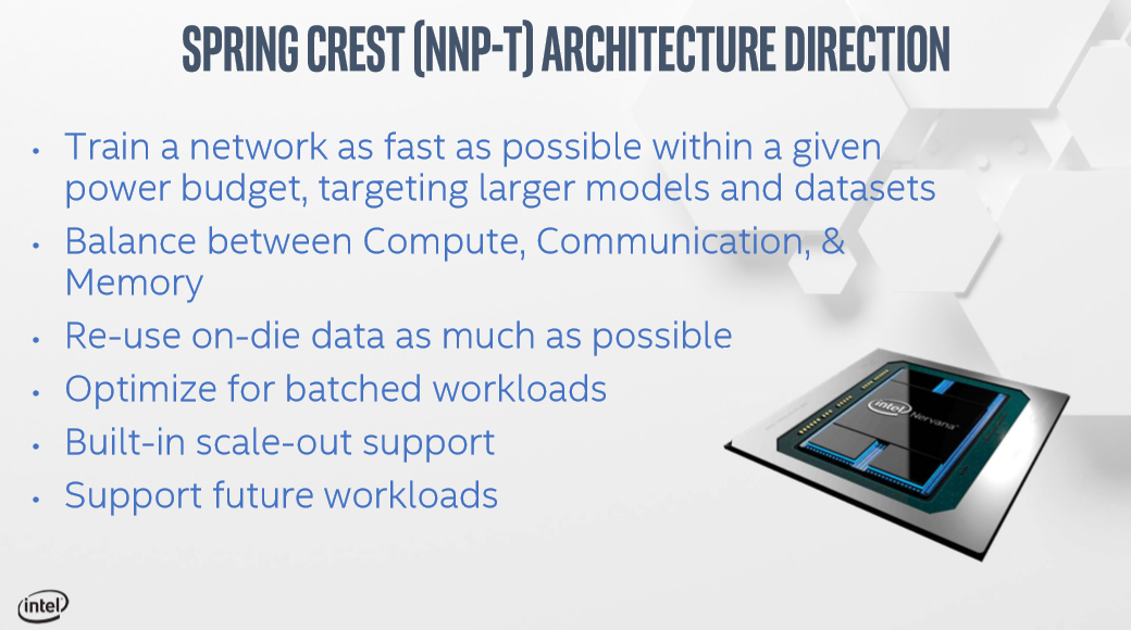
Enter the Spring Crest Deep Learning Accelerator, otherwise known as the Intel Nervana Neural Network Processor for Training (NNP-T), which is a mouthful no matter how you slice it. We'll stick to NNP-T.
This new accelerator comes as the fruit of Intel's acquisition of Nervana and represents a fundamental rethinking of the basic chip architecture to tailor it specifically for training workloads. More importantly, the Nervana architecture is tailored to scale workloads out to multiple cards, and even across multiple chassis, to the point that even rack-scale architectures based on the design could be a future direction. This design philosophy is important as the ever-expanding size and complexity of neural networks now have data center architects thinking of the chassis as the first unit of compute measurement, as opposed to the traditional paradigm of a single accelerator being the first unit of measure.
Accommodating the exploding size of the models, which Intel says are doubling roughly every five months, and complexity isn't just a function of boosting memory capacity/throughput and compute power: Both of those axes have to be paired with an efficient architecture that focuses on power efficiency, which is the ultimate measure of affordability in the data center. The design also requires a focus on an optimized communication system to reduce the power overhead associated with data traversal.
Get Tom's Hardware's best news and in-depth reviews, straight to your inbox.
The NNP-T SoC Architecture
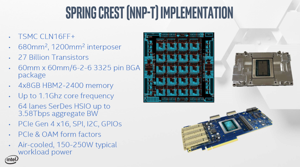
Here we can see Intel's take on the best approach to these challenges. The 688mm2 NNP-T die is fabbed on TSMC's 16nm CLN16FF+ process. It's a bit counter-intuitive to see a TSMC process on an Intel processor, but Nervana had already taped out its first-gen Lake Crest design on TSMC's 28nm processors before its acquisition by Intel, and continuing to use those design rules and TSMC's IP made sense to speed the transition to the current-gen Spring Crest product. Intel will also stick with TSMC for the next-gen model, but incorporate more of its own IP into the architecture, like power control and skewing technologies, creating what the company terms the "best of Intel and the best of Nervana."
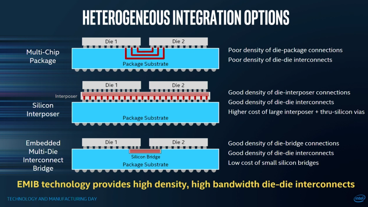
And the design uses plenty of TSMC's latest tech. The NNP-T die is flanked by four 8GB HBM2-2400 stacks (2.4 GB/s per pin) that all ride on top of a massive 1200mm2 silicon interposer. The die and HBM stacks are connected via TSMC's CoWoS (Chip-on-Wafer-on-Substrate) interconnect, which is a multi-chip packaging technique that uses micro-bumps to connect dies to a passive silicon interposer, which is then bonded to a package substrate that has through-silicon vias (TSVs). The result is a 60x60mm package that has a 3325-pin BGA interface (meaning it is not a socketed processor).
This is classified as a 2.5D packaging technology because the interposer is passive, while a similar design with an active interposer (active logic on the base die) would fall under the definition of 3D packaging. Meanwhile, the individual HBM2 stacks are true 3D implementations (4Hi). TSMC's CoWoS competes with Intel's own EMIB (Embedded Multi-die Interconnect Bridge) packaging that uses silicon bridges embedded into the package substrate.
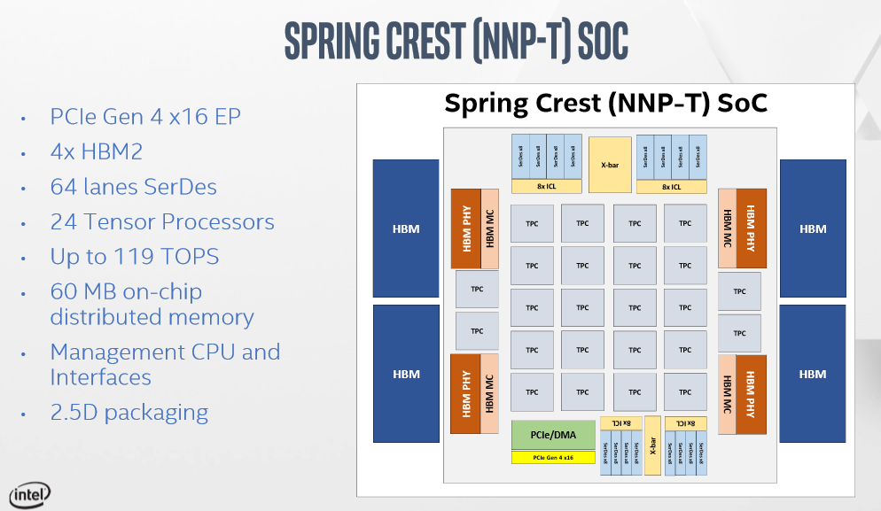
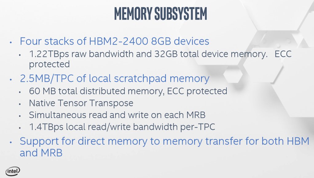
Fully utilizing the four HBM2 stacks required 64 SerDes lanes that support 28GB/s apiece (3.58Tbps aggregate). Those lanes feed the HBM PHY/memory controller on the die, which then routes data to the 24 Tensor Processors (TPC) located throughout the 27 billion-transistor die. The TCP's also house the 60MB of SRAM that is distributed throughout the die. There is also some die area dedicated to a management CPU and interfaces, like IPMI handling, I2C, and the like, along with 16 lanes of PCIe Gen 4.0.
The chip operates at 1.1 GHz and draws between 150 and 250W in air-cooled configurations, with more performance possibly unlocked with watercooling in the future. The NNP-T comes in OCP Accelerator Module (OAM) mezzanine card form factors (currently the hybrid cube mesh) due to their enhanced cooling and connectivity capabilities (seen here as the QFSP networking ports on the rear of the card). The OCP cards are experiencing a sharp uptake at hyperscale data centers, but the NNP-T also supports traditional PCIe card form factors.
Data In, Data Out
Having access to such prodigious memory throughput doesn't necessarily mean that you should use it all the time, largely because data movement is generally more expensive than compute in terms of power consumed and the time it takes for traversal. As such, minimizing data movement is a key ethos of the Nervana architecture.
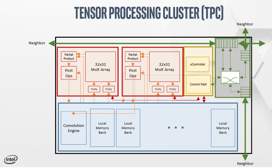
Diving into the Tensor Processing Cores finds several dual-ported memory banks that can read and write at the same time, and a Convolution Engine that can read data out of memory and convert it with convolutional filters to do matrix multiplies. The math happens in the red blocks, with the compound pipeline supporting pre-operations before the multiplies, and then multiple operations on the final product. The engine also outputs two operations at the same time, providing both the pre-operation and post-operation simultaneously. That minimizes the need for successive data movements through the compute pipeline. Intel also infused a small microcontroller (uController) directly into the control path that allows a custom instruction to trigger a subroutine in the microcontroller to perform specific operations.
Each TPC has four high-speed busses, with two dedicated to HBM2 memory while the other two handle communication with other TPCs.
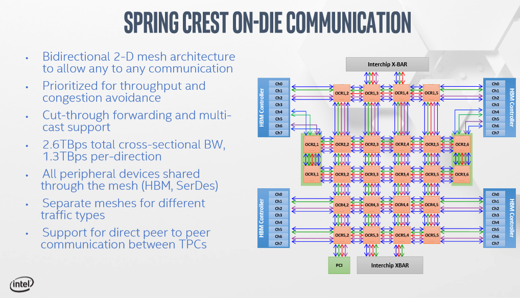
There is 60MB of SRAM spread across the TPCs. The TPCs are connected to the on-die network, which consists of a bi-directional 2D mesh architecture that has a separate bus that allows for data movement among the TPCs and can even move data off the die without accessing the HBM2 memory subsystem. This alleviates a common congestion point with read-heavy neural networks that require multiple accesses to HBM per operation, which creates a memory bottleneck that prevents the cores from being utilized fully.
Intel dedicates much of the die to a networking scheme that provides tremendous bandwidth both to and from the die (2.6Tbps total cross-sectional bandwidth). The mesh architecture has different networks for control, memory, die-to-die, and cluster-to-cluster communication (denoted by the colored arrows). This type of complex networking requires sophisticated routing and QoS (quality of service) controls to maximize throughput and avoid congestion. Unsurprisingly, many of Nervana's employees have deep backgrounds in networking technology, which helped in crafting the directly software-controlled send and receive architecture.
Raw Compute Power
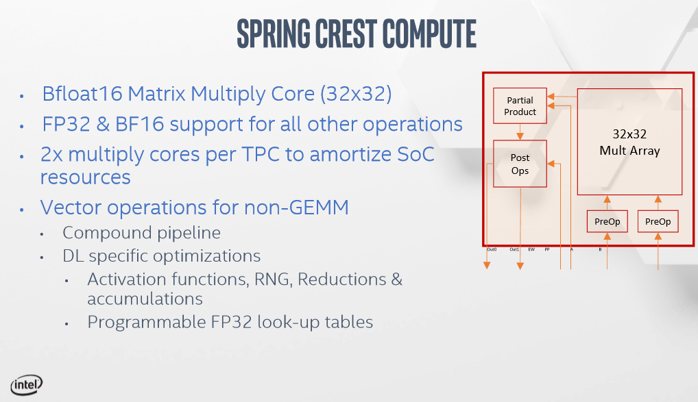
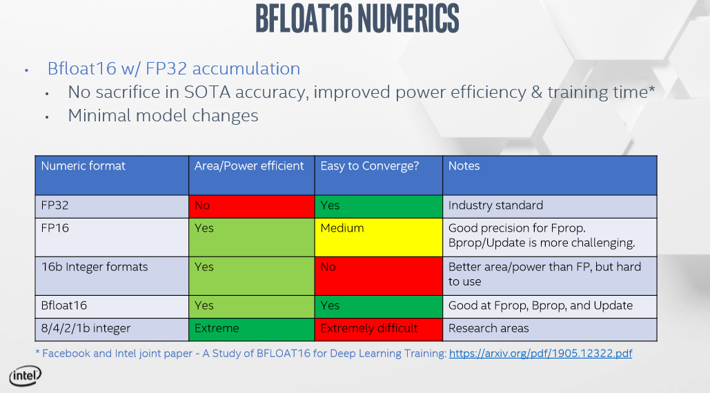
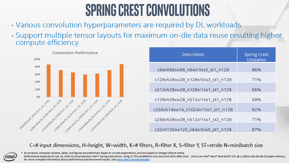
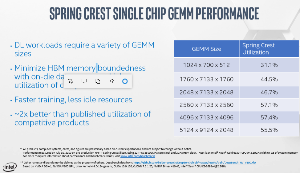
At the end of the day, maximizing performance of the memory and network subsystems helps to keep the cores fully utilized during data-heavy tensor workloads. Here we zoom in on the NNP-T's compute cores, two of which reside inside each TPC. The compute cores support bFloat16 matrix multiplies, FP32 and BF16, among all other major operations. Intel shared core utilization performance data with small message sizes, largely because competing architectures struggle at this metric, and also single-chip performance in deep learning workloads with various GEMM sizes. The utilization claims are far better than competing products, but as with all vendor-provided benchmarks, we'll have to wait for third-party analysis for the final verdict.
Performance at Scale
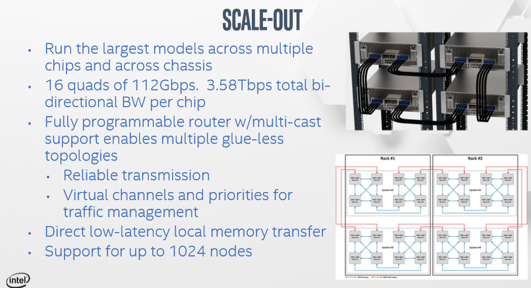
Spreading large models out among multiple chassis is a must, and the NNP-T is designed to scale gluelessly from chassis-to-chassis, and even rack-to-rack, without a switch. The network is designed with very high bandwidth and low latency in mind, which allows the architecture to handle massive models that scale to 5 or 8 billion parameters, or beyond.
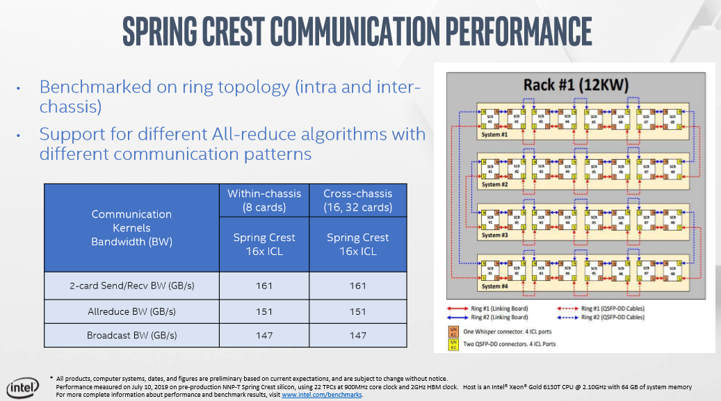
Intel also shared communication bandwidth performance data for the typical send/receive, but also measurements with Allreduce and Broadcast, which require computation between data transfers, to highlight the linear scaling from within the chassis to other chassis.
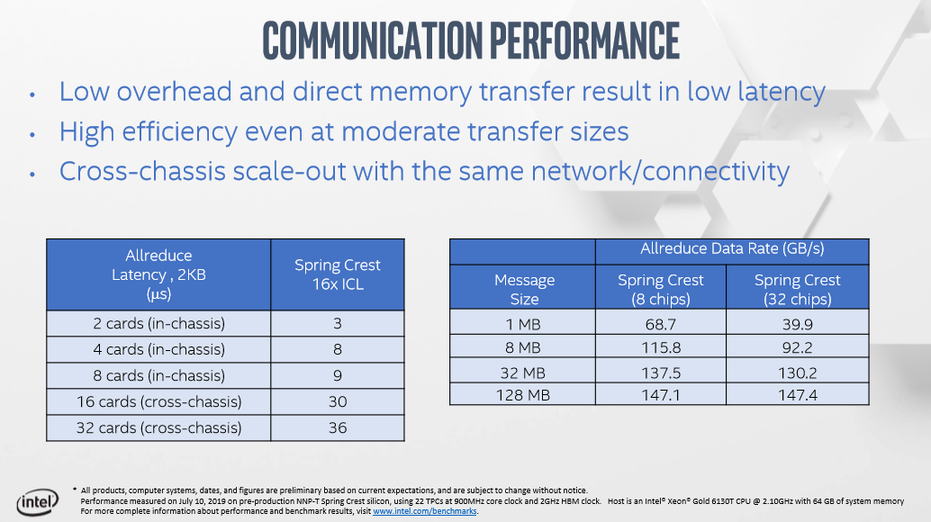
The company also provided latency metrics for different message sizes, with the small 2KB message sizes delivering exceptional latency characteristics and solid scaling up to 8MB message sizes. Again, this is latency measured in a real-world workload where there is computation involved between the steps, as opposed to standard performance measurements that only account for time on the link. Intel says it conducted these tests on its A-stepping silicon, while its B-stepping that will ship in final products should offer even better performance.
The architecture supports scaling to 1024 nodes with 8 NNP-T's apiece, but scaling and scaling efficiently are two different matters entirely. Intel hasn't published more expansive scaling efficiency testing numbers yet, but we're told the architecture scales well up to 256 cards, and perhaps beyond.
The Programming Model
Intel aims to abstract most of the software complexity away with the open-source nGraph library and compiler that connects frameworks to hardware back ends. Intel is working with Paddle Paddle, Pytorch, and TensorFlow frameworks.
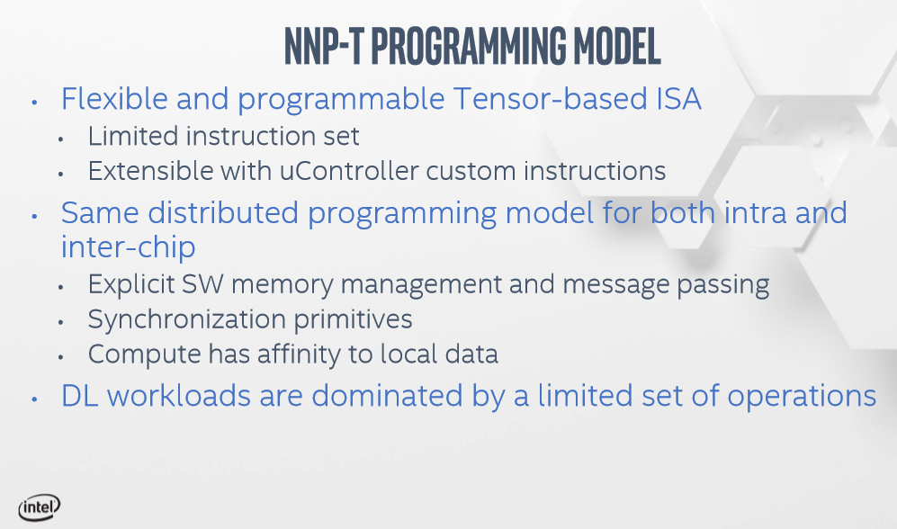
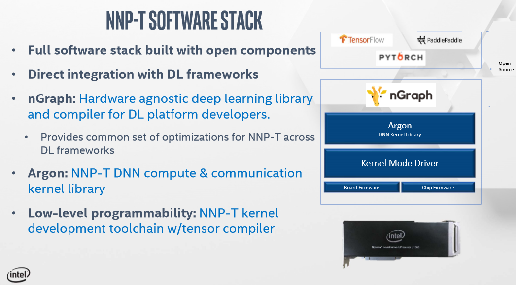
Tier 1 customers will get low-level access to the hardware, while 'broader' customers will get the kernel library. Intel will open up its own high-level programming language over the next year to allow customers to write their own kernels. The main goal here is simplicity, because complexity ultimately consumes die area. As a result, the custom ISA will be fairly simple to keep the die area focused on multipliers and memory. The company also has exclusive instructions for deep learning primitives.
Nervana NNP-T Ship Date
Intel says it will sample the NNP-T to leading-edge customers by the end of the year, with a specific focus on Tier 1 cloud service providers at first, and then opening the cards up to the broader market thought 2020. Intel says it already has the B-stepping silicon, which will ship in final products, running in its labs and that we should expect more updates over the next four months.

Paul Alcorn is the Editor-in-Chief for Tom's Hardware US. He also writes news and reviews on CPUs, storage, and enterprise hardware.
-
JayNor Nvidia already lost out on the end-all-be-all solution argument last year with the arrival of the crypto asic chips.Reply
We'll see if the ai asics similarly dominate ...
The bfloat16 support will be a low power advantage for the NNP-T.
The Microsoft Brainwave project indicates FPGAs are a win in some applications also. -
bit_user I had to smile at the PCIe 4.0 interface, since Intel won't have a CPU/platform capable of that until Q2 of 2020. So, in the meantime, I wonder how many of these will find their way into EPYC-based servers.Reply
The raw performance numbers don't strike me as anything that immediately threatens Nvidia, but they could have an edge in perf / W, multi-chassis scalability, and certain use cases.
What I expect to be their biggest challenge is that it's probably going to launch against the V100's successor, which should be on a 7 nm (possibly EUV) node. -
GetSmart Why Intel could not put HBM on normal CPUs? With 32GB HBM integrated, then don' t even need to buy memory kits.Reply -
bit_user Reply
I've been waiting for this and fully expected it to happen, by now. At least for ultra-mobile laptops or cell phones. Something with decent margins and integrated graphics, where the power savings would be at least on par with the performance gains.GetSmart said:Why Intel could not put HBM on normal CPUs? With 32GB HBM integrated, then don' t even need to buy memory kits.
Their final Xeon Phi (KNL) generation had 16 GB of MCDRAM, in package. And that launched at least 3 years ago, so...
Anyway, with Lakefield, they have finally got the DRAM in-package. Only 4-8 GB, though. -
GetSmart Reply
That MCDRAM is HMC type memory with high memory bandwidth but with memory latency similar to normal DDR3 or DDR4 memory. Wished Intel continued using these in their normal CPUs when their Intel Xeon Phi series got retired. Pretty sure there would be leftovers.bit_user said:Their final Xeon Phi (KNL) generation had 16 GB of MCDRAM, in package. And that launched at least 3 years ago, so...
This Intel Lakefield SoC would be very much at home in UMPCs, tablets, laptops (including Chromebooks), touch screen kiosks, compute sticks, SBCs (single board computers), ultra small mini PCs and drones. Kinda wondering if Intel is ever going to re-enter the mobile smartphone market again with this upcoming SoC.bit_user said:Anyway, with Lakefield, they have finally got the DRAM in-package. Only 4-8 GB, though. -
bit_user Reply
Sadly, bandwidth did not compare well vs. HBM, much less HBM2. But, if they'd stayed in it, maybe HMC2 would be better.GetSmart said:That MCDRAM is HMC type memory with high memory bandwidth but with memory latency similar to normal DDR3 or DDR4 memory. Wished Intel continued using these in their normal CPUs when their Intel Xeon Phi series got retired. Pretty sure there would be leftovers.
It has a 64 EU ("Iris Pro") GPU, however. So, that's a hint at which market(s) it's targeting. It will be a higher-margin part, where power-efficiency and form factor are at a premium. With only one "big" core, it's probably not going to target higher-end airtops, but with that 64 EU iGPU, it's not exactly destined for Chromebooks. And it makes no sense for NUCs, which don't need that level of integration or power-efficiency and wouldn't want to take the hit on big-core-count.GetSmart said:This Intel Lakefield SoC would be very much at home in UMPCs, tablets, laptops (including Chromebooks), touch screen kiosks, compute sticks, SBCs (single board computers), ultra small mini PCs and drones. Kinda wondering if Intel is ever going to re-enter the mobile smartphone market again with this upcoming SoC.
Of course, it could set the stage for things to come. And that where things could get really interesting.
