Intel Claims Sapphire Rapids up to 7X Faster Than AMD EPYC Genoa in AI and Other Workloads
AMX brings big AI performance gains.
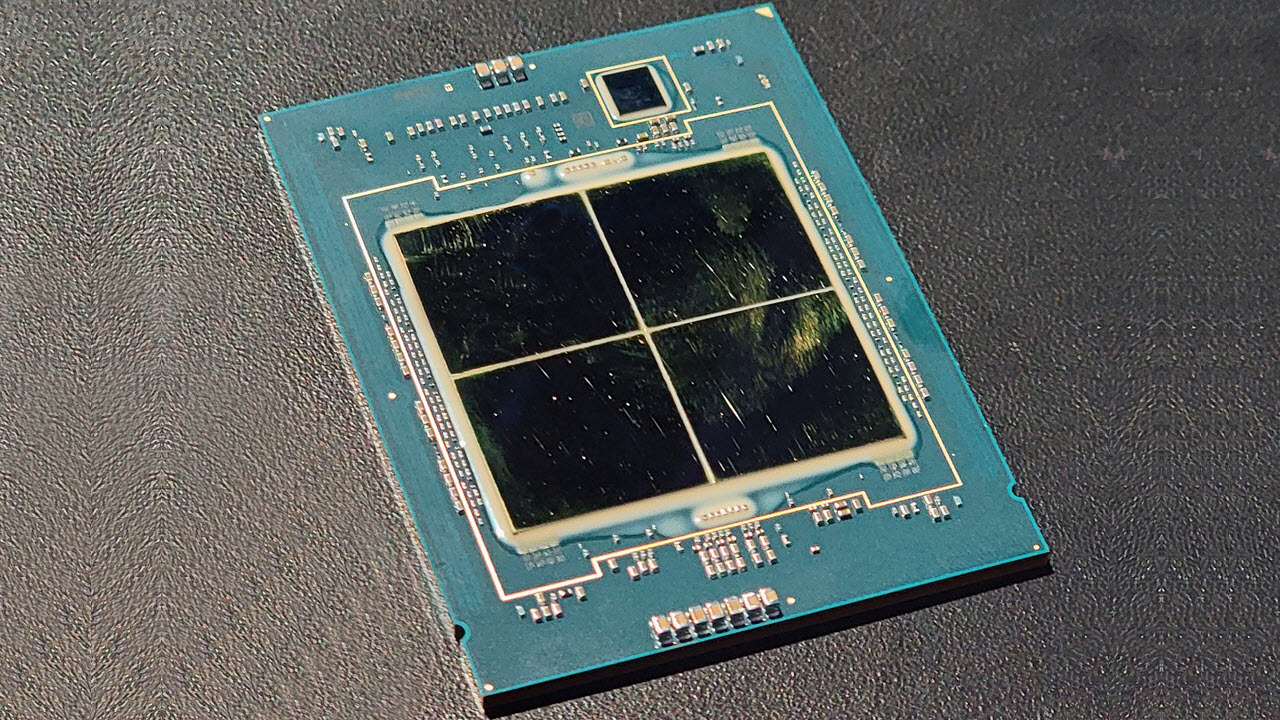
Intel has shared a slew of new benchmarks of its fourth-gen Xeon Scalable Sapphire Rapids CPUs going head-to-head with AMD's fourth-gen EPYC Genoa processors, claiming up to 7 times more performance in AI workloads when comparing two 32-core chips. Intel also touts higher performance under certain conditions, like when Sapphire Rapids' in-built accelerators are brought into play, in a spate of standard general-purpose workloads. Intel's 56-core Xeon Max, the first x86 data center CPU with HBM memory, also takes on AMD's 96-core flagship in several HPC workloads, matching or exceeding AMD's bulkier chip.
Intel's performance comparisons come well after the company's launch of its Sapphire Rapids Xeons back in January of this year, but the company says its benchmark comparisons were delayed due to difficulties procuring AMD's competing EPYC Genoa chips, which launched in November of last year. The benchmarks come a day before AMD's AI and Data Center event that we're flying out to cover, so we'll attempt to get AMD's feedback about Intel's benchmarks while we're at the event.
With a few shipping OEM systems powered by AMD's Genoa in hand, Intel has conducted a wide range of benchmarks in multiple types of workloads spanning AI, HPC, and general-purpose workloads, to present its view of the competitive landscape. However, as with all vendor-provided benchmarks, these should be approached with caution. Intel claims it enabled all rational optimizations for both its and AMD's silicon for these tests, but be aware that the comparisons can be a bit lopsided, which we'll call out where we see it. The price of the chips used for comparison are also lopsided, too. We've included Intel's full test notes for the tested configurations in the relevant image albums below. With that, let's take a closer look at Intel's results.
AI Workloads: Intel Sapphire Rapids Xeon vs AMD EPYC Genoa
For nearly every large organization, the question is no longer "if" or "when" they should deploy AI-driven applications into their deployments — the question is where and how. Yes, AI training remains the land of GPUs and various flavors of custom silicon, and we can expect Large Language Models (LLMs) to continue to rely upon those types of accelerators for the foreseeable future, but the majority of AI inference workloads still tend to run on CPUs. Given the quickening pace of AI infusion in the data center, the CPUs' performance in various types of inference will only become more important in the years to come.
Intel has had its eyes on accelerating AI workloads since the debut of its DL (Deep Learning) Boost suite with its second-gen Cascade Lake Xeon Scalable chips in 2019, which it claimed made them the first CPUs specifically optimized for AI workloads. Those chips came with support for new VNNI (Vector Neural Network Instructions) that optimized instructions for the smaller data types prized in AI applications. One of Intel's bedrock principles behind its AI strategy has been to use AVX-512 to vastly improve Xeon's performance and power efficiency in AI workloads by using VNNI and BF16. Intel's focus on AI acceleration features, including software optimizations, has expanded over the years to now include purpose-built AI acceleration engines on its Sapphire Rapids chips — if you're willing to pay the extra fee.
| Model | Price | Cores/Threads | Base/Boost (GHz) | TDP | L3 Cache (MB) | Memory | cTDP (W) |
|---|---|---|---|---|---|---|---|
| EPYC Genoa 9354 | $3,420 | 32 / 64 | 3.25 / 3.8 | 280W | 256 | 12-Channel DDR5-4800 | 240-300W |
| SPR Xeon 8462Y+ | $5,945 | 32 / 64 | 2.8 / 4.1 | 300W | 60 | 8-Channel DDR5-4800 | 270-300W |
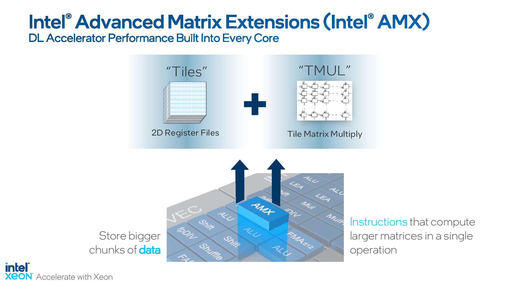
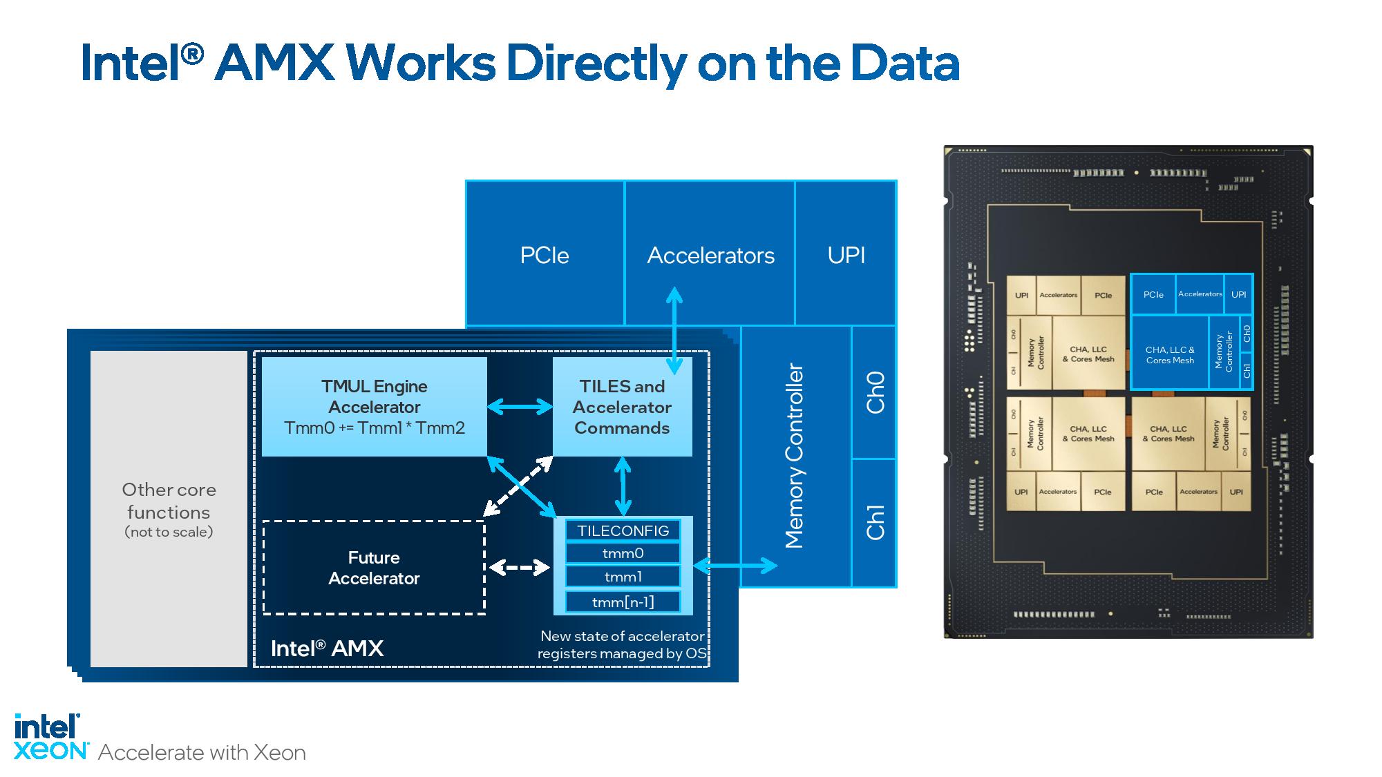
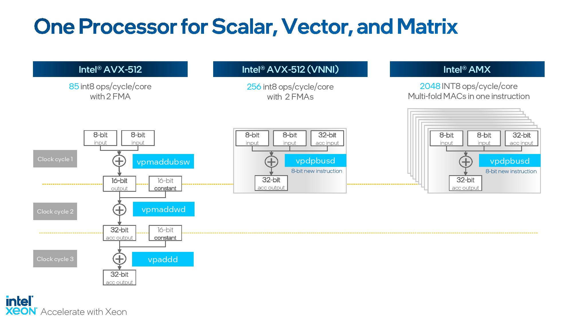
But a more important development lurks in the Sapphire Rapids silicon — Intel has now progressed to its new Advanced Matrix Extensions (AMX) x86 instructions, which deliver tremendous performance uplift in AI workloads by using a new set of two-dimensional registers called tiles. The Tile Matrix Multiply Unit (TMUL) that powers AMX is native to the Sapphire Rapids chips — you don't have to pay extra to use it like you do the dedicated AI accelerator engine — and leverages BF16 and INT8 to perform matrix multiply operations that can vastly enhance AI performance.
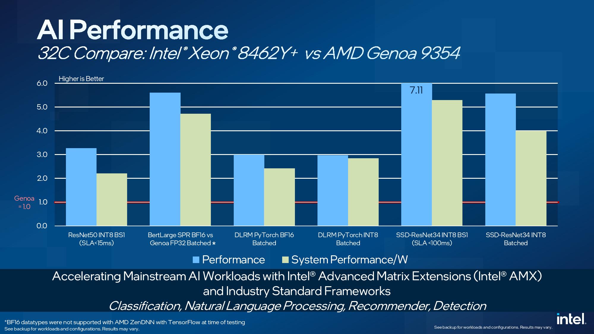
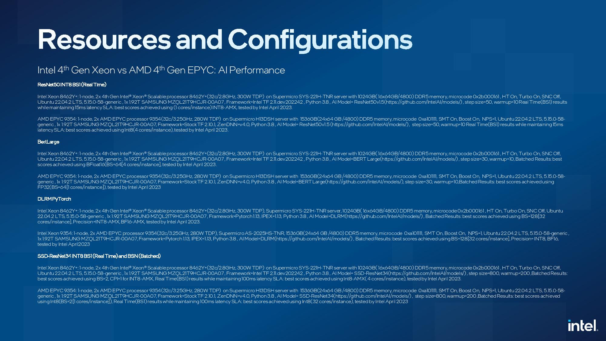
The benchmarks above leverage Intel's AMX, and not the optional in-built AI accelerator engine. Intel claims a 7X advantage over EPYC Genoa in ResNet34, a 34-layer object detection CNN model, using INT8 instructions at a batch size of 1 to measure latency — in this case, with an SLA of sub-100ms. Intel also claims a ~5.5X advantage in this same workload with a batched test. This model is trained in PyTorch but converted to the ONNX format.
Intel claims a ~3.3X advantage over AMD in ResNet50 (INT8 BS1) image classification with a sub-15ms SLA, and a 3X advantage in DLRM, a Deep Learning Recommendation Model, with PyTorch BF16 and INT8 in a batched workload.
We also see a ~5.5X advantage in BertLarge natural language processing with BF16, but that is versus Genoa with FP32, so it isn't an apples-to-apples test. Intel notes that BF16 datatypes were not supported with AMD's ZenDNN (Zen Deep Neural Network) library with TensorFlow at the time of testing, which leads to a data type mismatch in the BertLarge test. The remainder of the benchmarks used the same data types for both the Intel and AMD systems, but the test notes at the end of the above image album show some core-count-per-instance variations between the two tested configs -- we've followed up with Intel for more detail [EDIT: Intel responded that they swept across the various ratios to find the sweet spot of performance for both types of chips].
Overall, Intel claims that its AMX acceleration provides huge speedups in performance with industry-standard frameworks, but it's also important to call out the efficiency claims. The second yellow bar for each benchmark quantifies Intel's performance-per-watt claims, an incredibly important metric in today's power-constrained data centers — particularly with rising power costs in some climes, like the EU. Intel claims AMX delivers massive efficiency advantages when comparing two chips with similar core counts, which is surprising in light of Genoa's more advanced process node that tends to give it an efficiency advantage. Yes, dedicated silicon, as we see for AVX-512 and AMX, can be costly in terms of die area, and, thus, overall cost, but the advantages are huge if the applications can leverage the accelerators appropriately.
Intel's 32-core Xeon Platinum 8462Y+ chip squares off with AMD's 32-core EPYC Genoa 9354, but be aware that while these are iso-core-count comparisons, Intel lists the 8462Y+ for $5,945 while AMD lists the 9354 for $3,420, so the Intel chip costs 74% more. That said, the list pricing from both vendors is usually not reflective of what customers (particularly Tier 1 customers) actually pay, so take the pricing as a fuzzy guideline.
AMD does tend to offer higher core count chips at any given price point in the product stack and has a higher peak core count of 96 compared to Intel's 56 cores. Intel stuck with a 32-core vs 32-core comparison here, with per-core software licensing fees being the company's rationale for why these remain comparable. In fairness, software licensing, and other server BOM costs, like DDR5 memory and GPUs/accelerators, do have an outsized impact on solution-level pricing.
Given the size of Intel’s AI performance advantage with the 32-core parts, it’s reasonably safe to assume that it can compete with higher core count EPYC chips in these AI workloads, even if saddled with a reasonable amount of subpar workload/power scaling as they move to their own higher core count parts. Much of this performance can be chalked up to Intel's efforts on software enablement.
Intel doesn’t have any benchmark comparisons with LLMs (of the smaller variety), largely due to the raw and rapidly-changing nature of the LLM landscape. However, the company does say it is seeing impressive results with bandwidth-hungry LLMs on its HBM-equipped Xeon Max models (more below), which could be interesting given GPU shortages. We’re told that LLM benchmarks with Xeon Max will come in the future.
General Workloads: Intel Sapphire Rapids Xeon vs AMD EPYC Genoa
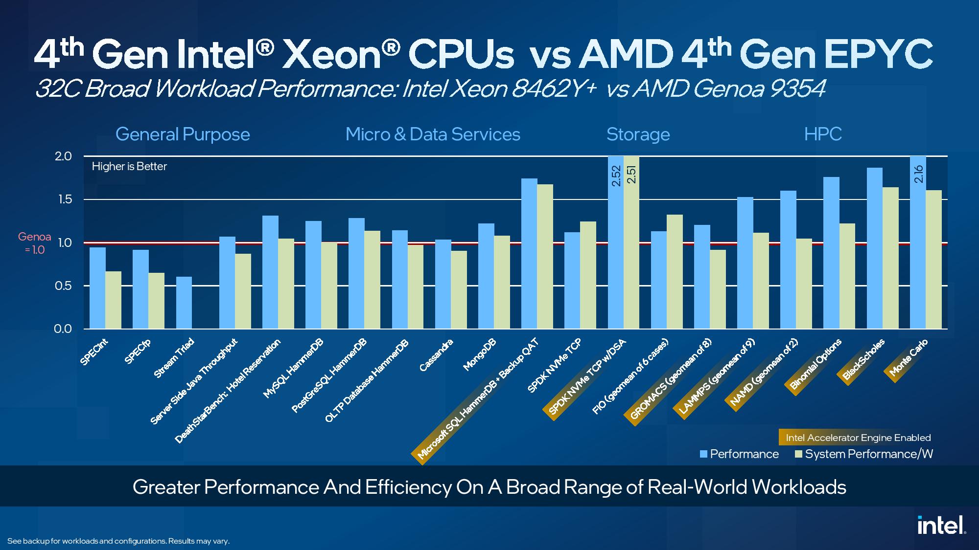
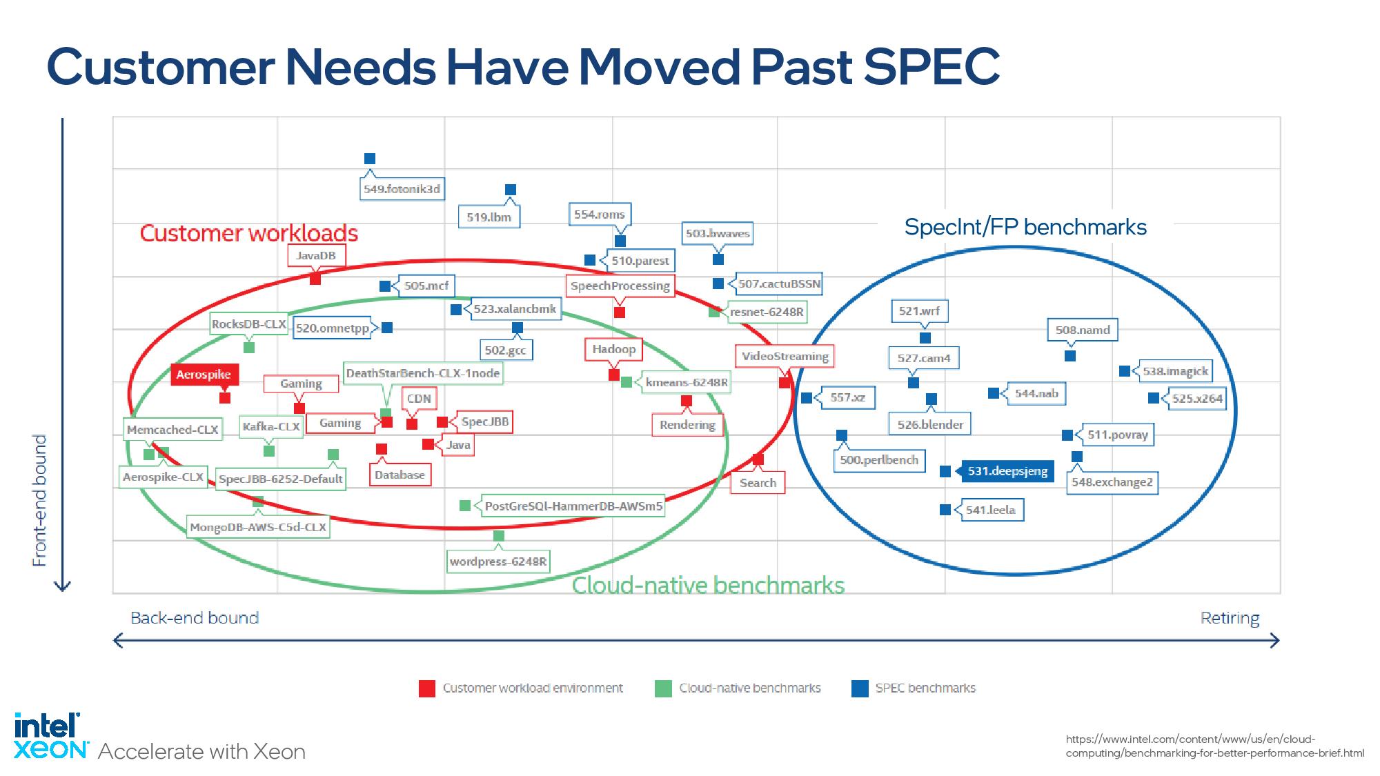
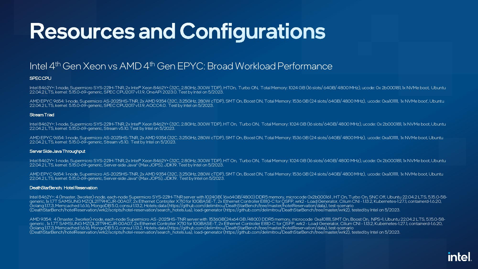
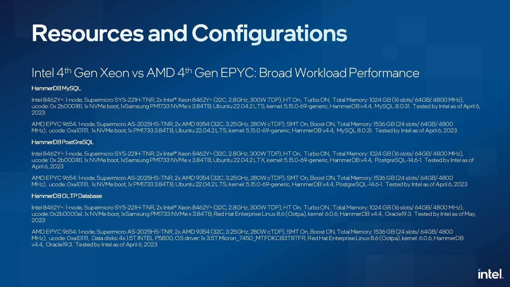
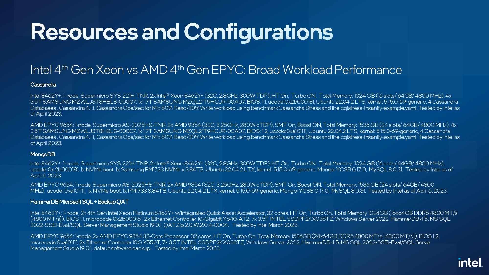
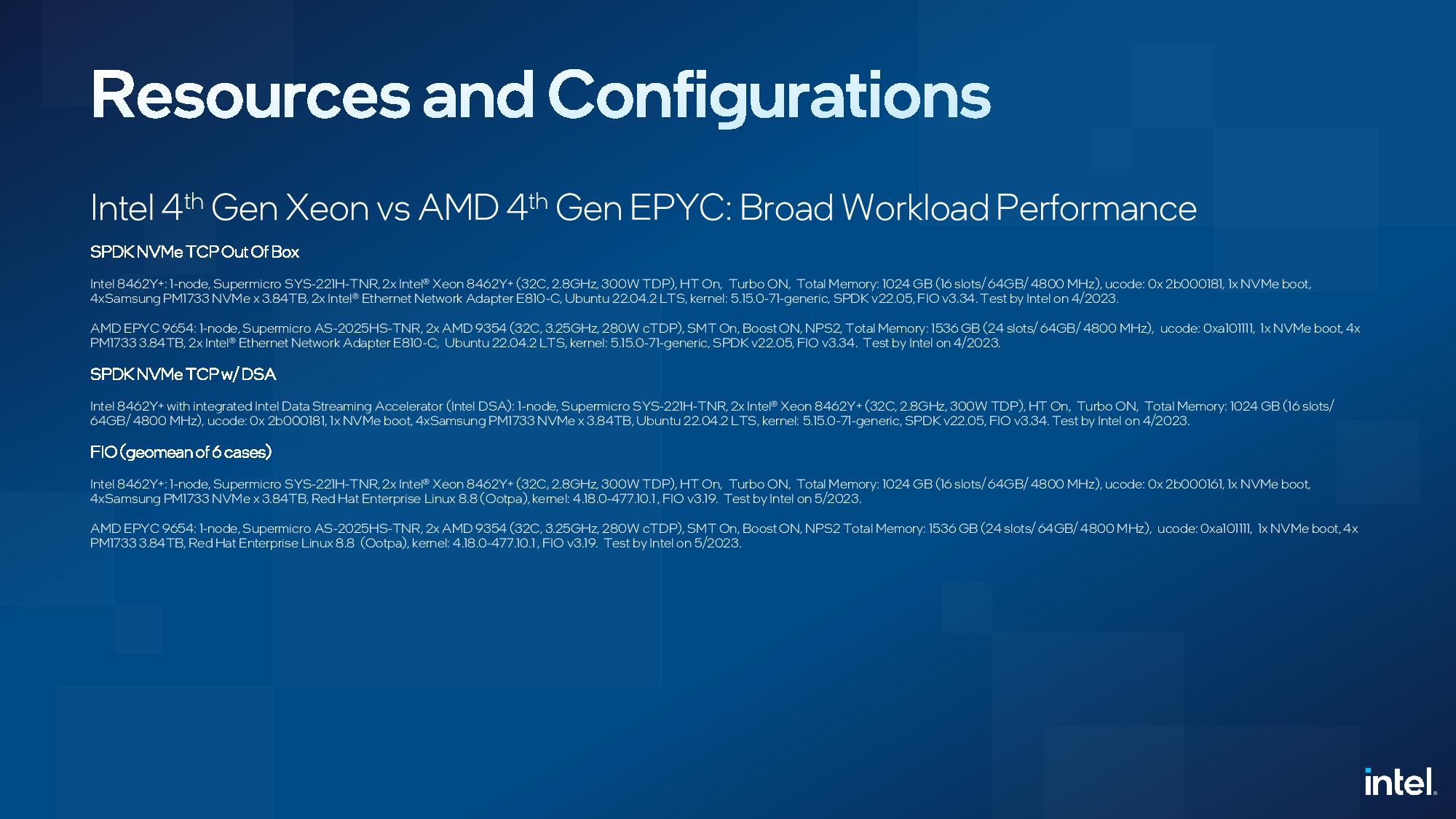
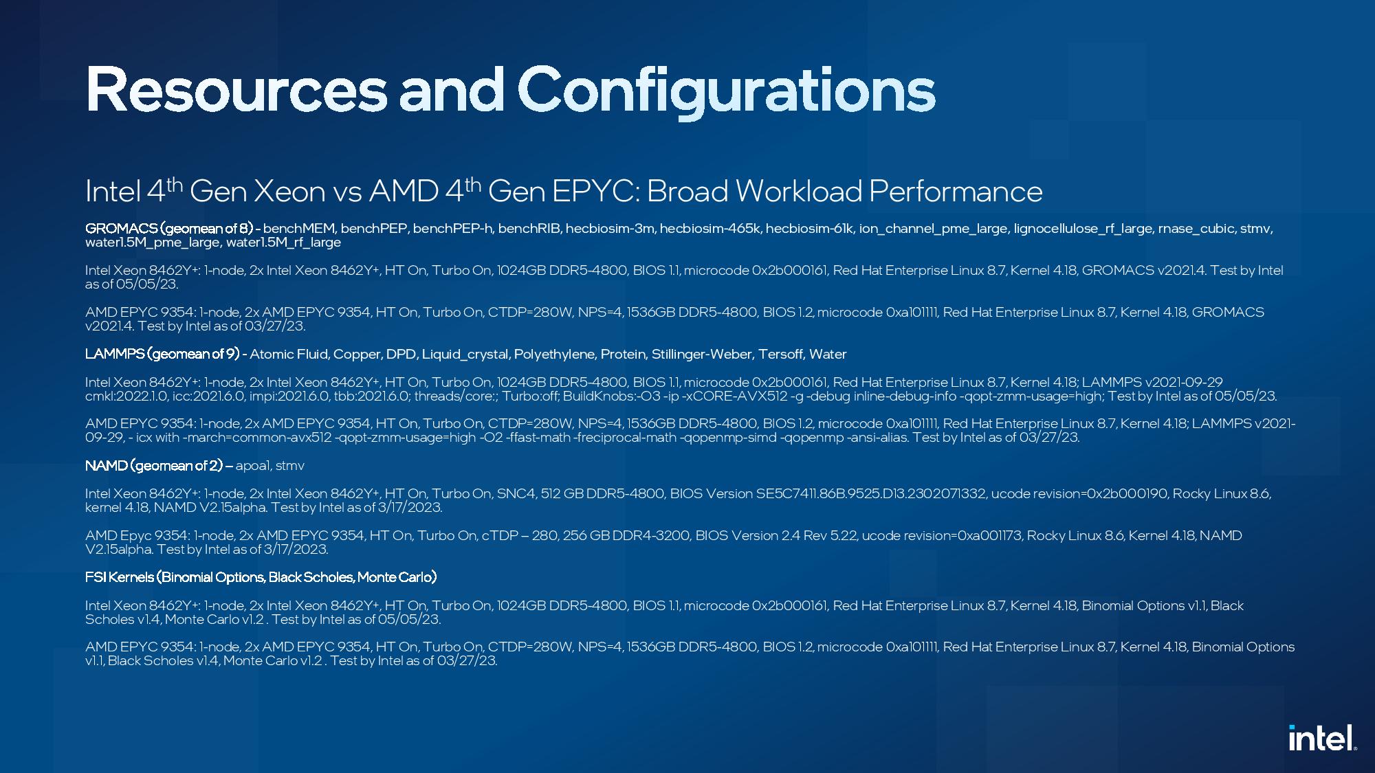
Here we see a standoff between the same two chips in a broader spate of general workloads. You'll note that Intel shows itself lagging Genoa in SPECint and SPECfp by large margins in efficiency and smaller margins in performance, but the company has recently begun de-emphasizing those industry-standard SPEC benchmarks because it feels the aging benchmark no longer represents real-world customer workloads -- that's actually not an uncommon viewpoint in the industry. Intel's take on SPEC is evidenced by the slideware they shared during the Sapphire Rapids briefings (second slide in above album). Intel says it is working on helping define the next generation of the venerable SPEC to make it more representative. For SPEC, Intel used the ICC compiler for Sapphire Rapids and AOCC for EPYC. The remainder of the benchmarks use 'mostly' the GCC compiler for both types of chips.
Intel also trails in the stream triad memory benchmark, which isn't surprising given that Sapphire Rapids has eight memory channels while Genoa has 12 (due to its higher channel count, AMD has 50% more memory capacity at its disposal in all of these benchmarks). That disparity also gives AMD an advantage in several other memory-bound workloads, like HPCG and Ansyst Fluent/Mechanical (not shown). It's clear that Intel is avoiding memory-bound workloads in these comparisons, though we do see those types of workloads in the HPC section where the company employs Xeon Max for comparison.
Intel largely claims slight performance gains in these workloads but notes that some of the larger gains come from employing its on-chip accelerator engines that require an extra fee to unlock. Intel used these engines in several of the workloads, marked in bronze on the horizontal axis, like SQL HammerDB, Gromacs, LAMMPs, NAMD, and others, to highlight the advantages of using the engines in tandem with applications that are tuned to exploit the advantages.
We haven't seen many benchmarks with these engines fully employed via software support, so it's clear that Intel is moving forward on the enablement front, and to good effect — at least according to its own benchmarks. Just be mindful that these accelerators, which speed AI, encryption/decryption, compression, data movement, and analytics, aren't available consistently across the Sapphire Rapids product stack and also cost extra.
There's also the matter of DPUs, too. These discrete accelerators can perform many of the same functions, such as encryption/decryption, compression, and data movement, at higher performance levels while also offloading the CPU, managing network traffic, and providing a separate control plane. Advanced DPU-augmented data center architectures aren't as widespread as the data center architectures that we consider 'traditional,' but that means the relative value of Intel's on-die accelerator engines will vary by deployment.
HPC Workloads : Intel Xeon Max vs AMD EPYC Genoa
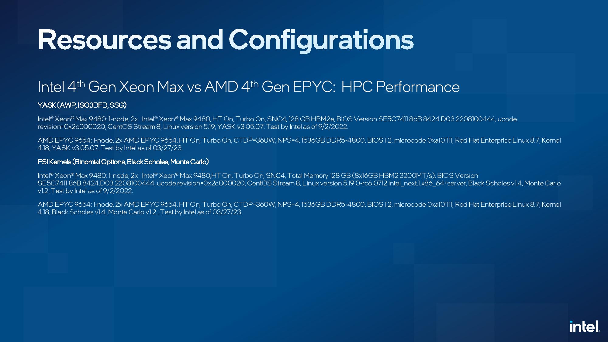
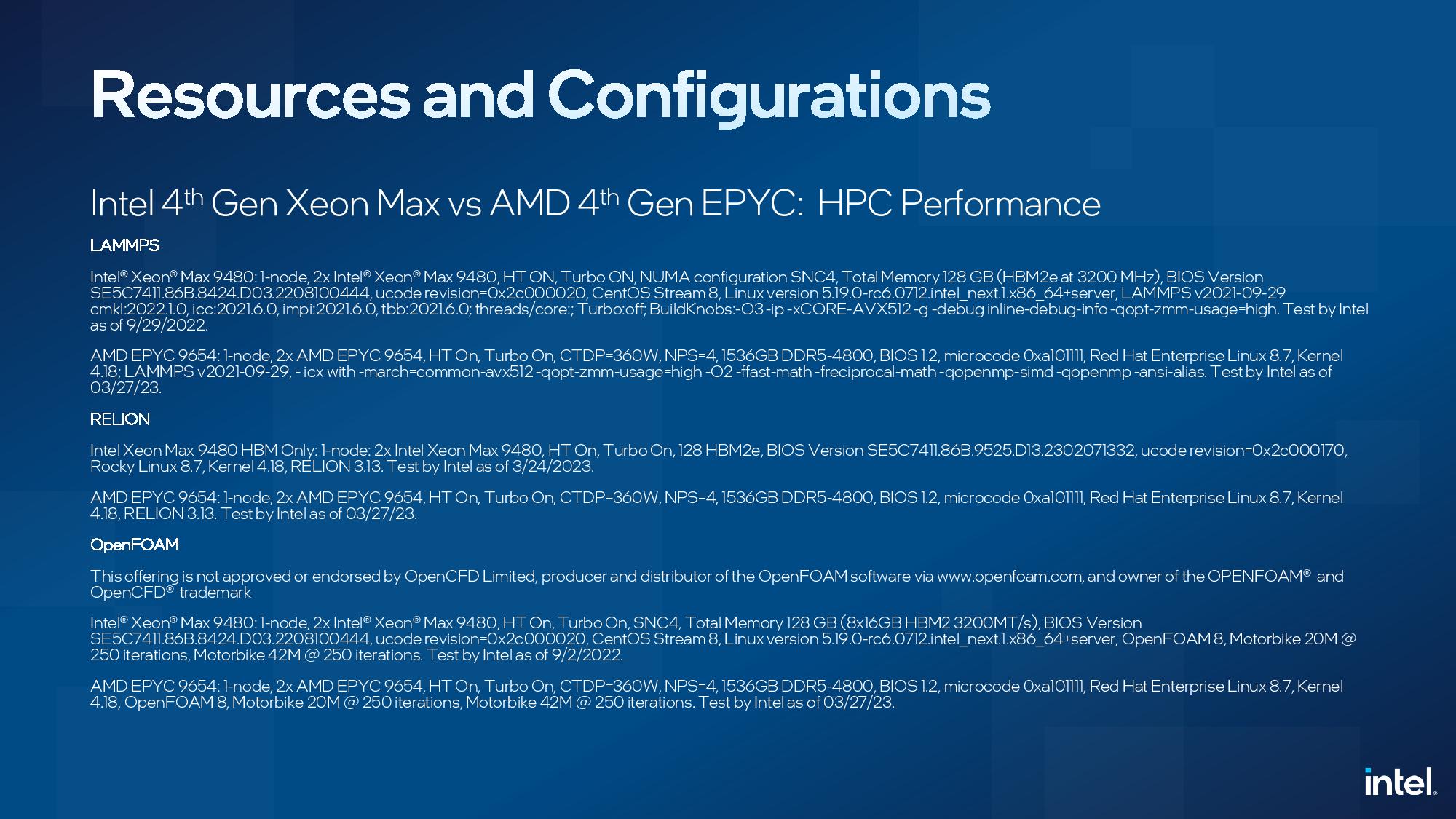
| Model | Price | Cores/Threads | HBM | Base/Boost (GHz) | TDP | L3 Cache (MB) | Memory | cTDP (W) |
|---|---|---|---|---|---|---|---|---|
| EPYC Genoa 9654 | $11,805 | 96 / 192 | n/a | 2.4 / 3.7 | 360W | 384 | 12-Channel DDR5-4800 | 320-400W |
| Xeon Max 9480 | $12,980 | 56 / 112 | 64 GB | 1.9 / 3.5 | 350W | 112.5 | 12-Channel DDR5-4800 | n/a |
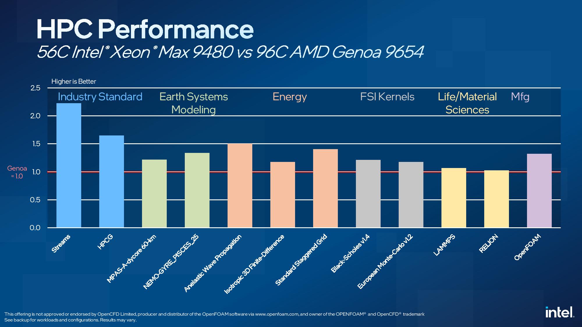
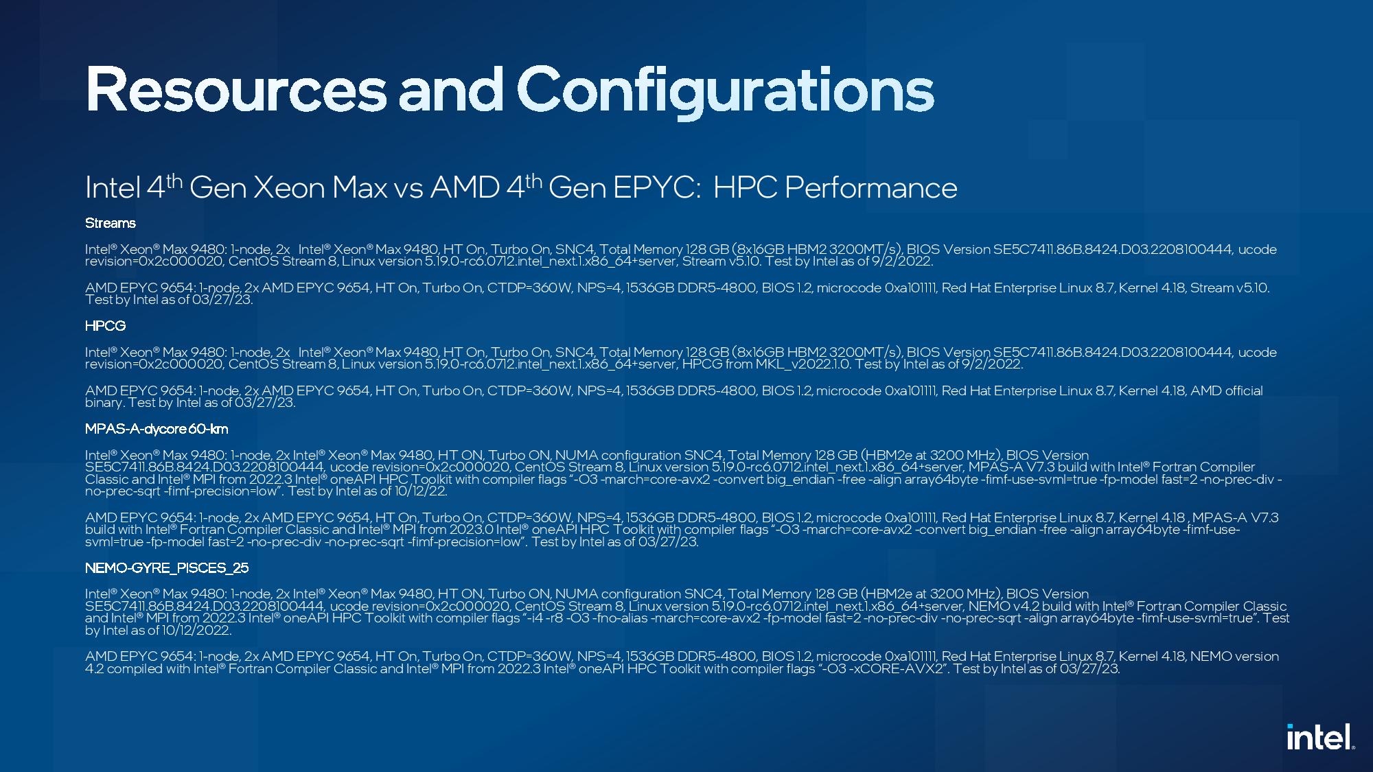
Here we see Intel's 56-core Xeon Max, the first x86 data center chip with on-package HBM to be pushed into full production, face off with AMD's 96-core EPYC Genoa flagship. Intel claims the onboard memory gives its smaller-but-not-less-expensive chip the advantage over the EPYC processor in a range of HPC-centric workloads, but without on-board accelerators enabled (oddly, only the data streaming accelerators are available on the Xeon Max models).
Naturally, these benchmarks won't land without plenty of dispute - there's a whole slew of architecture-specific optimizations possible for AMD's chips that could extract more performance, particularly in heavily-optimized HPC environments - but the key takeaway here is that Intel claims its HBM-equipped CPUs can offer compelling advantages in HPC that rival AMD's core-heavy flagships.
It is worth noting that both power scaling and chip fabrics can become a constraining factor with higher core-count chips in these types of workloads. As such, it's conceivable that some of these workloads could shift to a more favorable outcome for AMD with a slightly less prodigious model, like its own 64- or 56-core Genoa’s. Also, Intel's chips here only use the HBM2e memory -- there is no DDR5 attached. As such, AMD's Genoa has a tremendous memory capacity advantage (1.5TB of DDR5 capacity vs 128GB of HBM2e capacity for Xeon Max).
AMD has taken somewhat of a different path of augmenting its chips with extra memory by 3D-stacking the L3 cache for its Milan-X processors, and we expect the company to announce its newer Genoa-X chips tomorrow at its event tomorrow. However, AMD gears Milan-X for certain technical workloads, as opposed to positioning it for the broader HPC market as Intel does for Xeon Max.
TCO: Intel Sapphire Rapids Xeon vs AMD EPYC Genoa
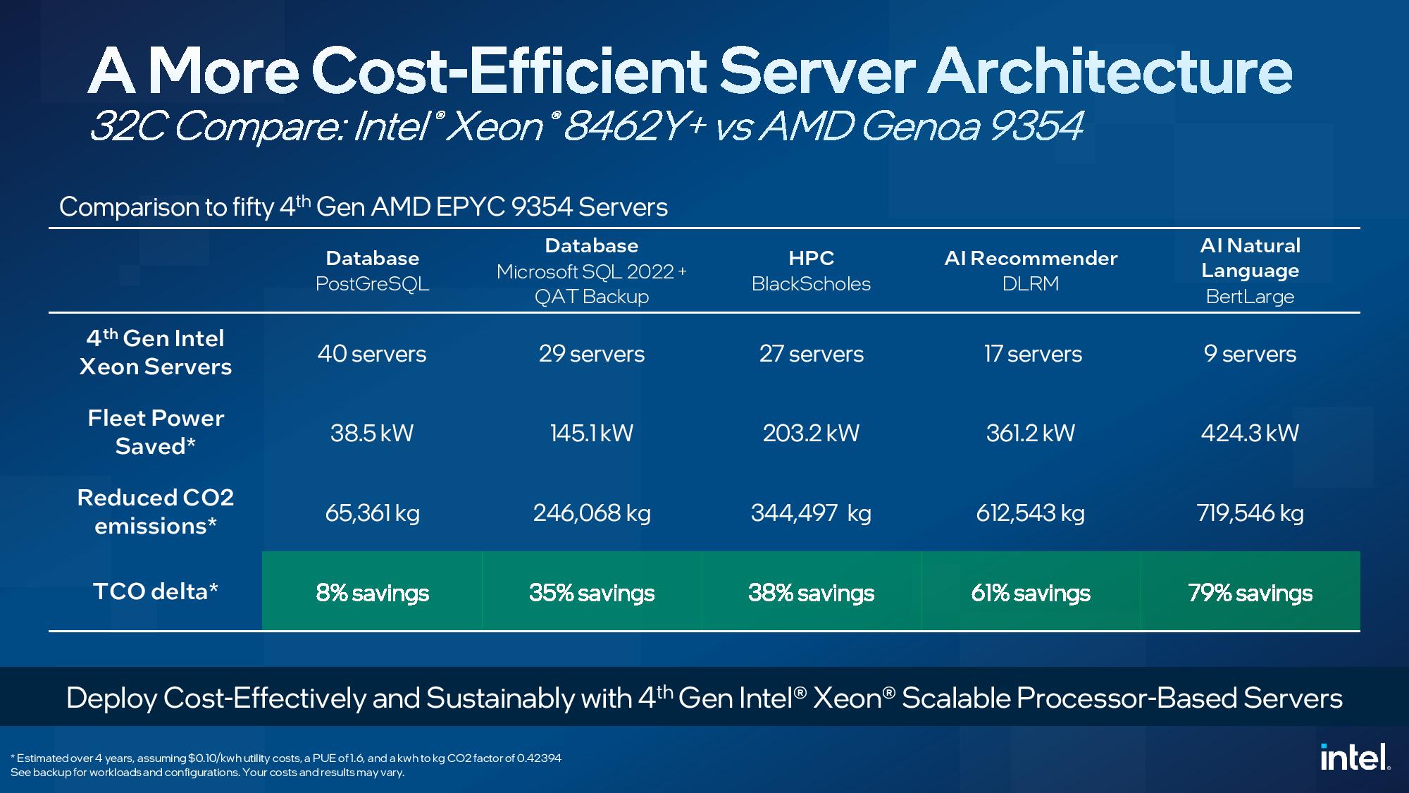
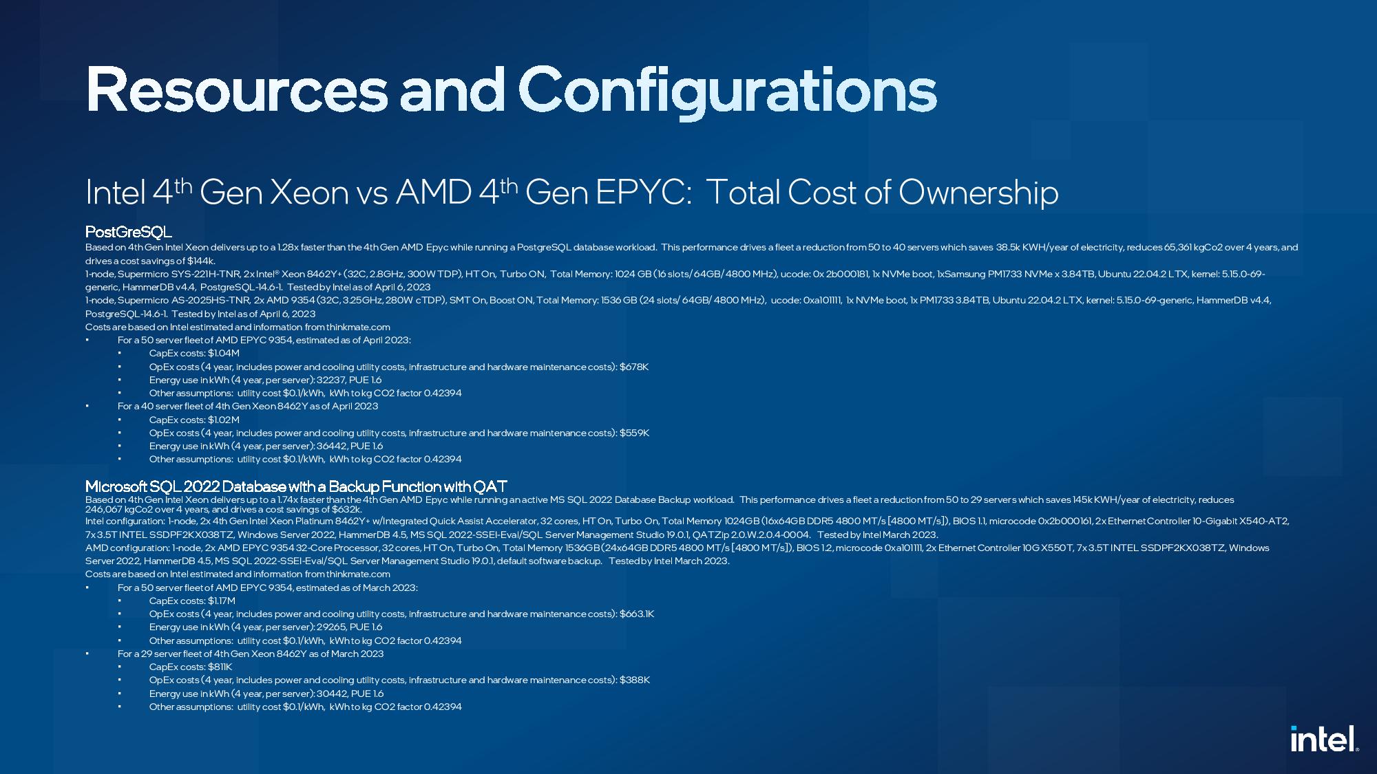
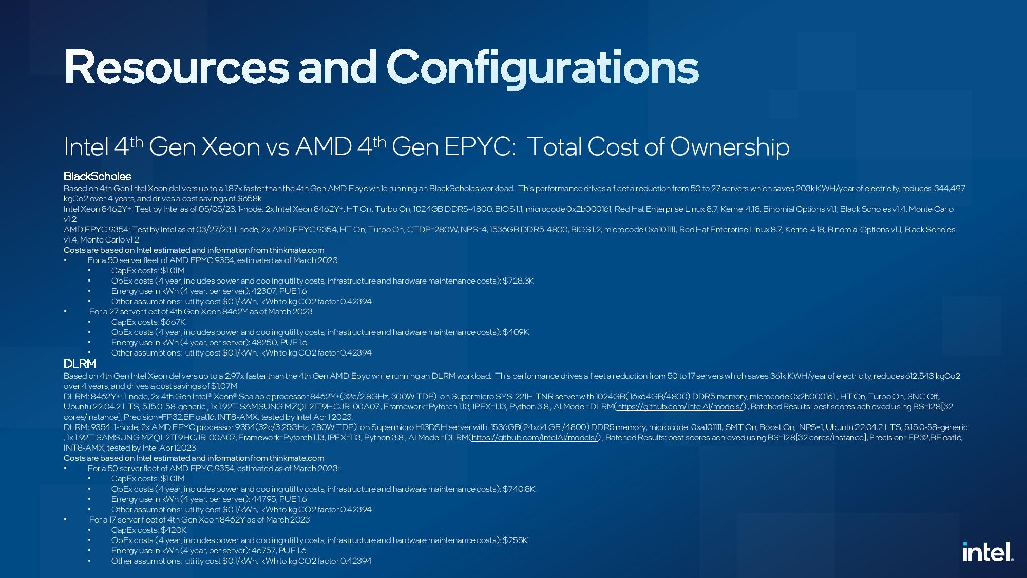
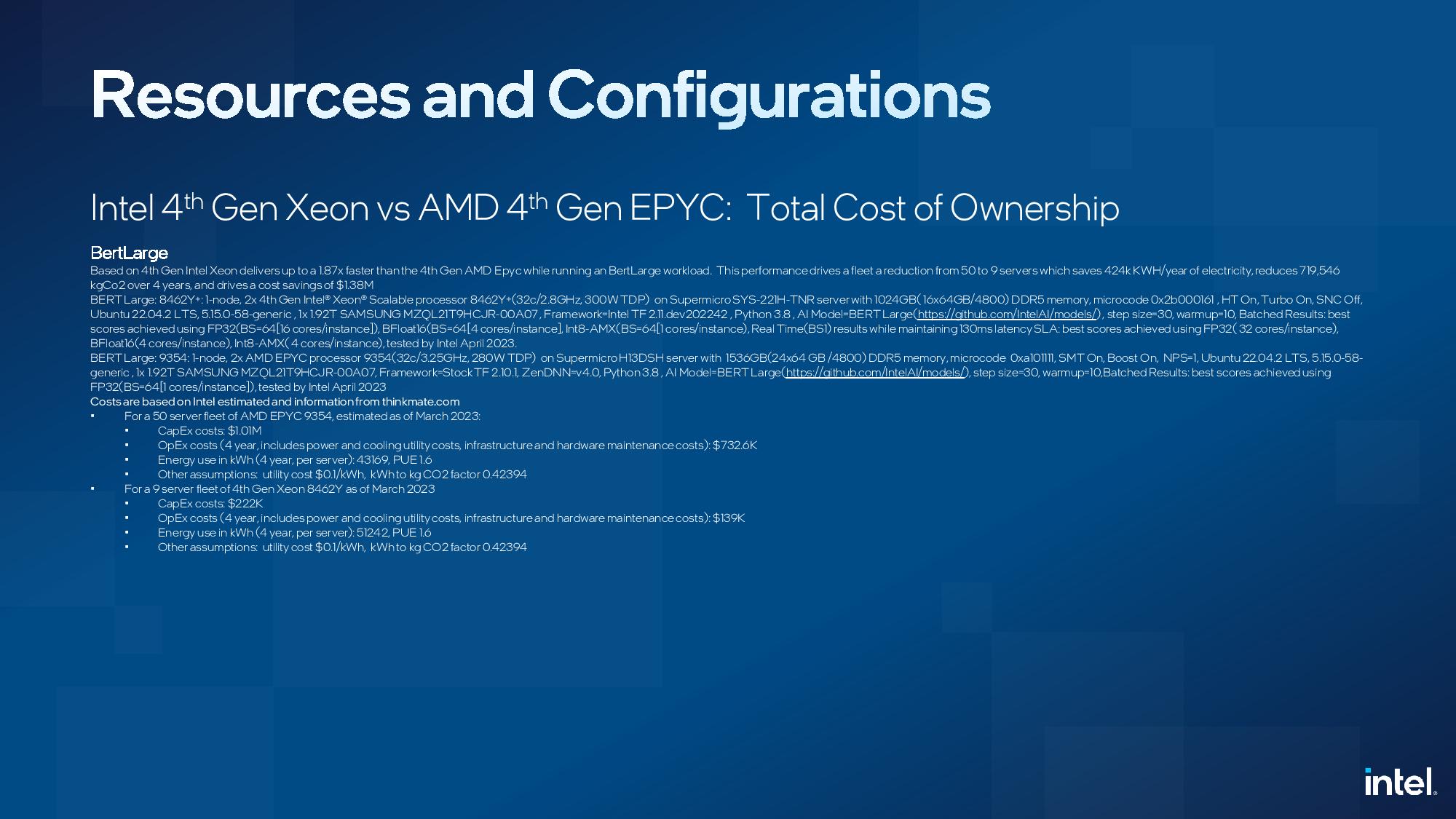
Every vendor has its own take on how to calculate the Total Cost of Ownership (TCO), but they're all typically questionable -- overall TCO will vary so widely by deployment that it's truly hard to derive solid metrics that are indicative of broader trends.
Intel's take is that using the SPEC benchmark for deriving TCO values isn't indicative of real-world use cases, which we touched on briefly in the general workloads section above. As such, Intel provides a range of examples here for different types of deployments, and the associated savings of using Intel chips over AMD's EPYC. Some of these comparisons, like the QAT backup, aren't much better than using SPEC, so take them with a big grain of salt and be sure to check the configuration slides we've included in the album.
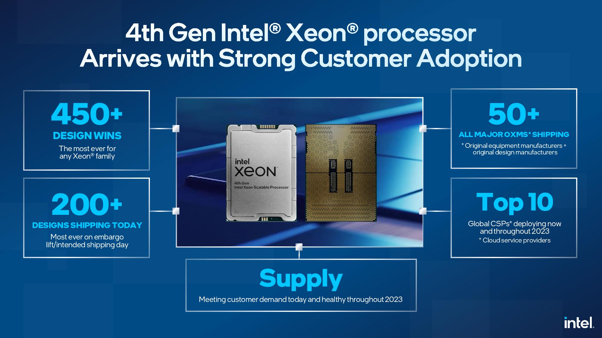
Intel also points to an accelerating pace of deployment, with 200 designs of 450+ Sapphire Rapids design wins already shipping. Intel also points out that it already has cloud instances in general availability at Google Cloud (notably paired with its Mount Evans IPU/DPU), and preview instances already available at several other cloud providers, like AWS. In contrast, AMD has yet to have any publicly available Genoa instances in the US, preview or otherwise, at cloud providers (we are aware of public instances available in China). We'll inquire about the status of AMD's cloud efforts at its event tomorrow and update as necessary.
Get Tom's Hardware's best news and in-depth reviews, straight to your inbox.
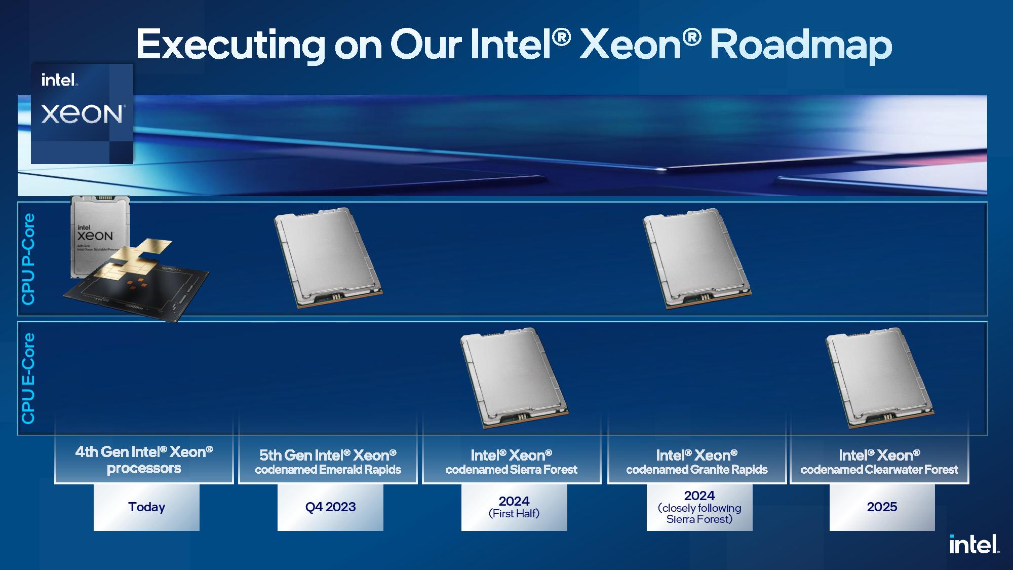
Finally, Intel reiterates that its recently-revised data center roadmap remains on track, which you can read about here. We have a few questions still pending with Intel about the above benchmark test configurations, and will add more info as it becomes available.

Paul Alcorn is the Editor-in-Chief for Tom's Hardware US. He also writes news and reviews on CPUs, storage, and enterprise hardware.
-
FWIW, the compiler side of the initial AMX enablement work was already started in GCC 11, and has also been part of LLVM 12 since its late 2020 release. That being said, AMX is just a matrix math overlay for the AVX-512 vector math units.Reply
More like a “TensorCore” type unit for the CPU. -
rtoaht AMD needs an answer to the AI accelerators. With the advent of generative AI, it is now mainstream.Reply -
lightofhonor Reply
Their new 7040 chips have AI accelerators built-in. Not hard to imagine their EPYC line will get this sometime too.rtoaht said:AMD needs an answer to the AI accelerators. With the advent of generative AI, it is now mainstream. -
Tech0000 AMX is, so far, only BF16 and INT8 data types matrix multiplications and nothing else (technically dot product).Reply
BUT it is foundational with more variations coming in the pipeline (reading intel's doc) FP16 etc
They are also talking about complex valued data types in Granite Rapids etc.
What makes matrix multiplications so important in AI is that it is the most complex component in the inner most loop in training, dominating the compute complexity and, importantly, memory bandwidth.
By reducing the Matrix multiplication to a handful of assembly instructions
1 tile load instruction: Throughput/Latency = 8/45
1 tile multiplication instruction: Throughput/Latency = 16/52
1 tile store (result): Throughput/Latency = 16
you achieve reduction in over all latency and throughput (magnitudes):
1. you only read the source matrix data once (not multiple times like when using any other method AVX, AVX2, AVX512...)
2. the compute clock cycle latency of 8+16+16 = 40 clock cycles for a tile multiplication (a small 16x16 matrix) is an order of magnitude faster than any other method on a CPUs
it is incredibly good use of silicon for AI apps. -
waltc3 If Intel's marketing was a reflection of its hardware and sales, AMD would be lost...;) Fortunately for AMD, that's not the case...;)Reply -
bit_user AI WorkloadsFirst off, there's simply no way a CPU without a comparable matrix-multiply can compete with AMX. So, let's get that out of the way, up front. Of course, for heavy AI workloads, I don't expect most people to be using a CPU as their main AI compute engine. Note that they're not comparing against GPUs or other AI accelerators!Reply
Credit to @PaulAlcorn , as I had noted the same things but he was already ahead of me:
"We also see a ~5.5X advantage in BertLarge natural language processing with BF16, but that is versus Genoa with FP32, so it isn't an apples-to-apples test. Intel notes that BF16 datatypes were not supported with AMD's ZenDNN (Zen Deep Neural Network) library with TensorFlow at the time of testing, which leads to a data type mismatch in the BertLarge test. The remainder of the benchmarks used the same data types for both the Intel and AMD systems, but the test notes at the end of the above image album show some core-count-per-instance variations between the two tested configs -- we've followed up with Intel for more detail ."
Further observations:
Used Genoa with 2 DIMMs per channel (see end notes) - doesn't that incur a speed penalty? Also equipped Xeon with 2 DIMMs per channel. I wonder if the penalty is as much?
Genoa had NPS=1 (NPS=4 typically yields better performance).
Of course, they're using CPUs with the same core-count, when one of the main selling points of Genoa is that it has more cores.
Regarding that last point:
"per-core software licensing fees being the company's rationale for why these remain comparable."
None of the software in their benchmarks has per-core licensing. I'm pretty sure it's all open source, even.
General WorkloadsI don't have much to say here, except that AMD is clearly using higher core-counts in opposition to Intel's increased reliance on accelerators. So, it seems logical to use another factor, like price, to determine which CPUs to match up to each other.
Also, where specified, most tests used NPS=1, except for the FIO test, GROMACS, and LAMMPS.
Finally, some of the tests used RHEL or Rocky Linux, with a 4.18 kernel. You really have to wonder how many of the more recent optimizations got backported to these ancient kernels, for the respective CPUs.
HPC WorkloadsIn this category, it would be really nice to have AMD's 3D V-cache equipped CPUs, but I guess they still have yet to launch the Genoa version? Maybe AMD is planning to do that at the Tuesday event.
Again, I'm struck by how many of these benchmarks used an ancient 4.18 kernel. I would expect HPC users to be a lot more interested in running newer kernels, in order to extract the most performance from their massive hardware and energy expenditures. Not only that, but such old distros won't have the compiler optimizations needed to enable features like AVX-512 on Genoa. However, in some cases, they do seem to make a point of compiling with AVX2 on both CPUs.
I'm pleased to see NPS=4, on all cases except Stream. I guess they felt they had enough bandwidth to spare, that they could allow this. -
bit_user Reply
That actually makes sense, relative to when Sapphire Rapids was supposed to launch.Metal Messiah. said:FWIW, the compiler side of the initial AMX enablement work was already started in GCC 11, and has also been part of LLVM 12 since its late 2020 release.
FWIW, I think it really doesn't make much difference when they started building it into compilers, because it's not really the type of feature that I'd expect a compiler to automatically utilize. You'd have to explicitly insert intrinsics into your code, if you want the compiler to perform these ops, although maybe the compiler at least manages the registers for you?
At least 99% of users will be simply utilizing it through a handful of libraries optimized by Intel, so it won't matter much if they had to write them in assembly language or what.
😵💫Metal Messiah. said:That being said, AMX is just a matrix math overlay for the AVX-512 vector math units.
No, I'm pretty sure it's not.
Intel claims it has far higher narrow (int8) FMA throughput:
Here, Locuza shows us it takes a real chunk of die space in each Sapphire Rapids version of Golden Cove:
Source: https://locuza.substack.com/p/info-snack-alder-lake-m-raptor-lake
And it adds 8x 1 kB tile ISA registers, which could theoretically be implemented via overlays on the same register pool used for ZMM registers, but I sure doubt it! Given that AMX has its own logic, and no instructions for direct interchange with the ZMM registers, it wouldn't be very practical to use the same underlying registers.
Where did you even hear that? In all I've read about AMX, I've never come across such a statement.
What's funny is that it's even more like an actual core than Nvidia's Tensor cores. They actually do use the same CUDA registers as their SIMD instructions. In both Nvidia and Intel's case their dispatched from the same instruction stream, making neither a proper core in its own right.Metal Messiah. said:More like a “TensorCore” type unit for the CPU.
https://www.anandtech.com/show/12673/titan-v-deep-learning-deep-dive/3 -
JayNor AMX has its own operations, storage, and register files.Reply
See the fuse.wikichip info from article June, 29, 2020, titled "The x86 Advanced Matrix Extension (AMX) Brings Matrix Operations; To Debut with Sapphire Rapids" -
bit_user Reply
AMD's response is clear: integrate CPU and GPU dies (with HBM) into the same package:rtoaht said:AMD needs an answer to the AI accelerators. With the advent of generative AI, it is now mainstream.
https://www.tomshardware.com/news/new-amd-instinct-mi300-details-emerge-debuts-in-2-exaflop-el-capitan-supercomputer