Intel Talks Falcon Shores Flub, Merges Habana Gaudi Roadmap
Falcon Shores, take two!
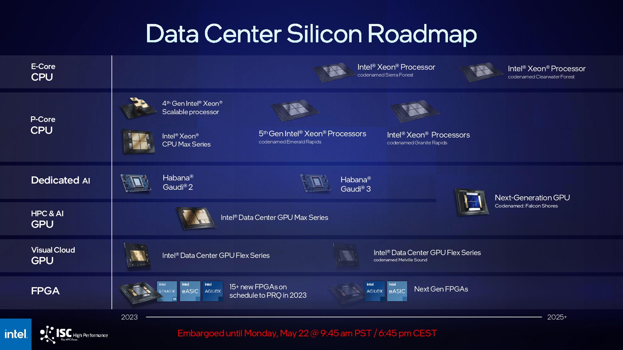
Intel originally planned for its Falcon Shores chips to have both GPU and CPU cores under the hood, creating the company's first 'XPU' for high performance computing. However, its surprise announcement a few months ago that it would pivot to a GPU-only design and delay the chips to 2025 left industry observers shocked — this leaves Intel unable to compete with AMD's Instinct MI300 and Nvidia's Grace Hopper processors that both feature a blended CPU+GPU design.
Today Intel provided some of its somewhat questionable rationale behind the decision to pare back its plans for Falcon Shores to make it the GPU-only successor to the Xeon Max GPU series. Intel also sketched out some of the early details of its new GPU-only Falcon Shores design, which we'll cover further below.
Intel also issued a new HPC and AI roadmap that doesn't show a successor to the Gaudi3 processor — instead, Gaudi and GPUs merge with the Falcon Shores GPU as it takes on the mantle of Intel's premiere HPC and AI chip. Intel told us that it 'plans to integrate the Habana and AXG product [GPU] roadmaps,' but the details of the integration are slight.
The Gaudi compute architecture varies significantly from a standard GPU, so it doesn't appear that its compute architecture could be entirely integrated into the GPUs. As such, Intel could be incorporating smaller parts of the Gaudi design, like its networking interface or other IP blocks, into its GPUs. We're told that Jeff McVeigh, the VP and GM of Intel's Accelerated Computing Group, will provide further details today. As a reminder, Intel paid $2 billion for Habana Labs and killed off products from its $350 million Nervana acquisition to focus on the Gaudi chips.
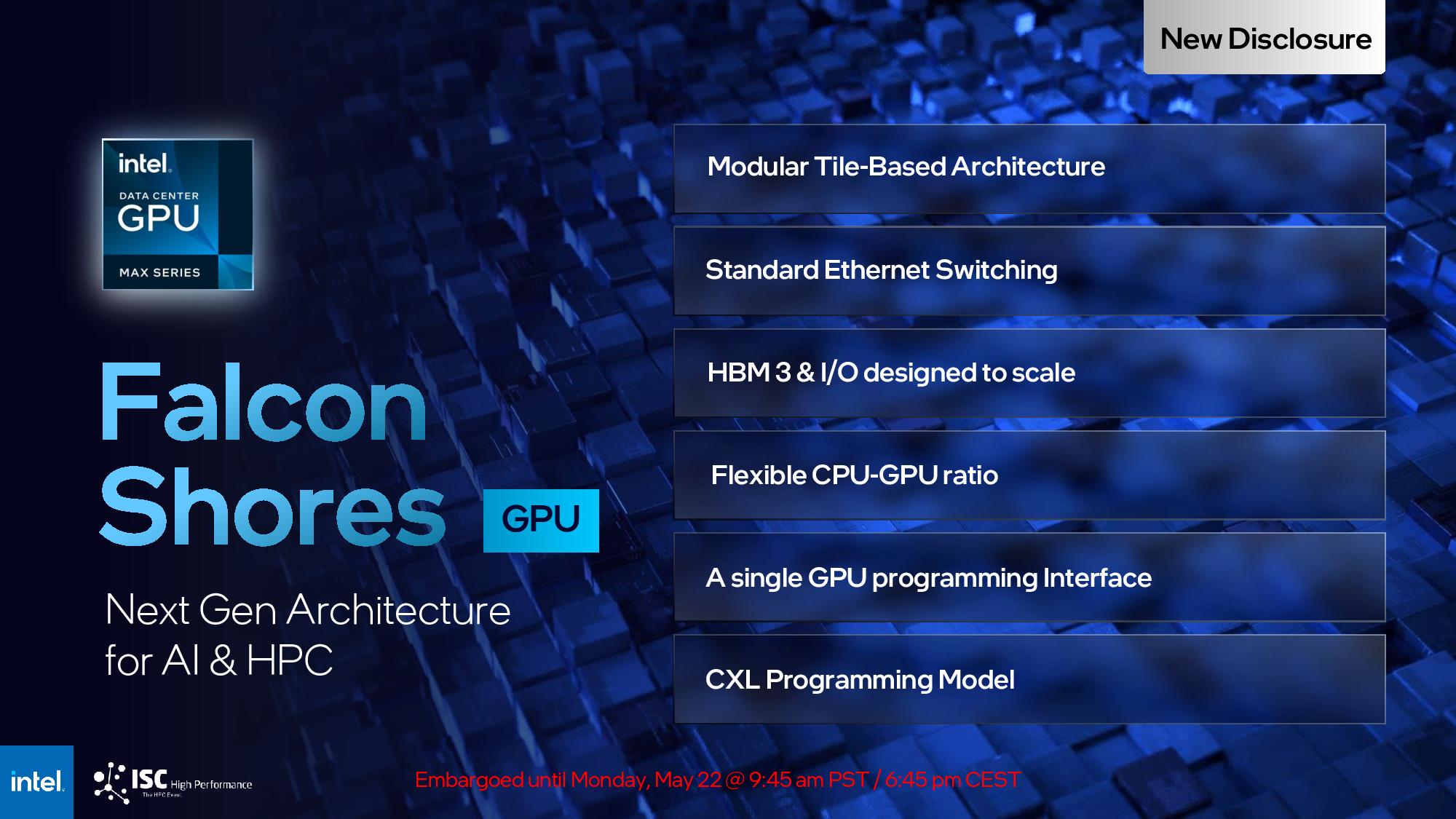
Intel shared some basic details about the new Falcon Shores design, which will continue to focus on HPC and AI workloads but will employ GPU cores. The HPC-focused Falcon Shores XPUs were designed for supercomputing applications with plans to merge both CPU and GPU technology into one mix-and-match chip package, but they will now first arrive as a GPU-only architecture in 2025.
Falcon Shores will employ standard ethernet switching, much like Intel's AI-focused Gaudi architecture, an unspecified amount of HBM3 memory, and "I/O designed to scale," likely signifying that Falcon Shores will come with different memory capacity options. Intel does say that Falcon will come with up to 288GB of HBM3 and 9.8 TB/s of total memory throughput. As expected, it will support smaller data types, like FP8 and BF16.
The basic sketch of the device also includes a common GPU-based programming interface, OneAPI, that will allow broad compatibility with other CPUs and architectures. Intel also lists CXL support as a key differentiator, which brings us to its rationale behind yanking the CPU cores from the Falcon Shores package.
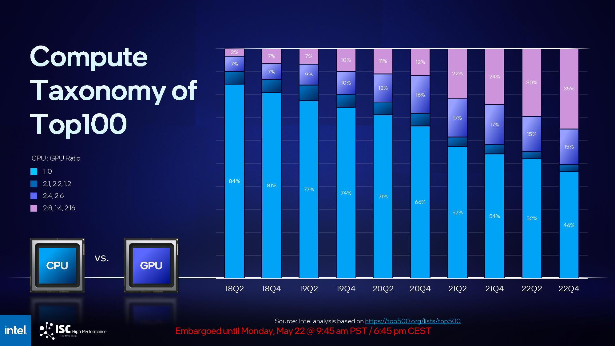
Intel says that its initial goal of mixing CPU and GPU cores into the same Falcon Shores package was premature. As shown in the above slide, Intel says that the optimum mix of CPU and GPU cores has shifted over time as workloads have evolved, and the company expects even more rapid and radical changes to the optimum CPU/GPU ratio to occur with the explosion of generative AI and LLMs into the HPC space. As such, Intel says it doesn't feel that the time is right to lock customers into specific CPU and GPU ratios.


However, as shown above, the original plan for Falcon Shores did include the ability to adjust CPU/GPU ratios by dropping in a different number of either CPU or GPU tiles into the four-tile design, thus allowing it to configure the optimum blend for various workloads. Besides, by design, supercomputers on the leading edge are highly specialized designs for the task at hand, and software tuning for the architecture is simply a routine part of the business of operating a supercomputer. These factors imply that CPU/GPU ratios aren't the only reason Intel removed CPU cores from the design.
Intel also points to allowing its customers to use various different CPUs, which would logically include AMD's x86 and Nvidia's Arm chips, with their GPU design, thus not locking customers into choosing Intel's x86 cores over other companies. But, again, Intel's original plans also included GPU- and CPU-only variants of Falcon Shores, so this rationale also doesn't seem convincing.
Intel says it will leverage the CXL interface to allow its customers to leverage a composable architecture that can tie together various CPU/GPU ratios in their custom designs. However, the CXL interface provides only 64 GB/s of throughput between elements, while custom CPU+GPU designs like Nvidia's Grace Hopper can provide up to 1 TB/s of memory throughput between the CPU and GPU. That confers both performance and efficiency advantages over a CXL implementation for many types of workloads — especially memory bandwidth-hungry AI workloads. That's not to mention the inherently lower-latency connections between elements and other advantages, like higher performance density.
That is to say that while Intel's idea of a more composable architecture is fine for some workloads, it will likely not be able to compete with AMD's MI300 or Nvidia's Grace in power, cost, or performance for certain applications.
Likewise, Intel's decision to slow its GPU release cadence isn't ideal as it will have to leverage older products to compete with far more advanced architectures for HPC, like Nvidia's Grace Superchips and AMD's coming exascale APU, the Instinct MI300, that both launch in 2023.
Despite Intel's rationale for changing its goals, it's hard not to see Intel's redefinition of Falcon Shores into a GPU-only product as the company missing an architectural inflection point that will put it at a competitive disadvantage in the future.
Get Tom's Hardware's best news and in-depth reviews, straight to your inbox.

Paul Alcorn is the Editor-in-Chief for Tom's Hardware US. He also writes news and reviews on CPUs, storage, and enterprise hardware.
-
JayNor "However, the CXL interface provides only 64 GB/s of throughput between elements"Reply
based on what limitation in CXL?
Are you saying, based on a 16 lane PCIE5 bus? -
JayNor The IPUs are taking over a lot of traditionally CPU owned territory. Perhaps Intel is getting schooled by google on the GPU only design of the initial Falcon Shores.Reply
No mention yet of optical, which was hinted by R. Koduri. -
I think it is up to 64 GB/s in each direction over 16 lanes.Reply
32GT/s x16 for CXL 2.0
64GT/s x16 for CXL 3.0 -
PlaneInTheSky lol @ the AI product lineReply
"We're going to sell lots of AI chips! ...right John?"
"I think it was a fad"
"a fad?! what about all those people using Bing with chatGPT?"
"No one is using Bing sir" -
JayNor Diamond Rapids is expected in 2025 timeframe, and with PCIE6/CXL 3.0 according to some leaks. It would make sense to delay the GPU a year to introduce the new CXL and PCIE6, if that's what they're doing.Reply