Nvidia Details Grace Hopper CPU Superchip Design: 144 Cores on 4N TSMC Process
Nvidia shares more details at Hot Chips 34.
Nvidia announced new details about its Grace CPU Superchip in advance of its Hot Chips 34 presentation next week, revealing that the chips come fabbed on the 4N process. Nvidia also shared more information about the architecture and data fabric, along with more performance and efficiency benchmarks. Nvidia hasn't made its official presentation at Hot Chips yet — we'll add the finer-grained details after the session — but the information shared today gives us the broad strokes as the Grace chips and servers work their way to market in the first half of 2023.
As a quick reminder, Nvidia's Grace CPU is the company's first CPU-only Arm chip designed for the data center and comes as two chips on one motherboard, totaling 144 cores, while the Grace Hopper Superchip combines a Hopper GPU and the Grace CPU on the same board.
Among the most important disclosures, Nvidia finally officially confirmed that the Grace CPUs use the TSMC 4N process. TSMC lists the "N4" 4nm process under its 5nm node family, describing it as an enhanced version of the 5nm node. Nvidia uses a specialized variant of this node, dubbed '4N,' that is optimized specifically for its GPUs and CPUs.
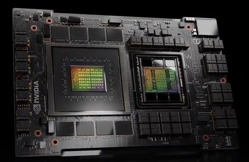
These types of specialized nodes are becoming more common as Moore's Law wanes and shrinking the transistors becomes harder and more expensive with each new node. To enable custom process nodes like Nvidia's 4N, chip designers and foundries work hand-in-hand by using Design-Technology Co-Optimization (DTCO) to dial in custom power, performance, and area (PPA) characteristics for their specific products.
Nvidia has previously revealed that it uses off-the-shelf Arm Neoverse cores for its Grace CPUs, but the company still hasn't specified which specific version it uses. However, Nvidia has disclosed that Grace uses Arm v9 cores and supports SVE2, and the Neoverse N2 platform is Arm's first IP to support Arm v9 and extensions like SVE2. The N2 Perseus platform comes as a 5nm design (remember, N4 is in TSMC's 5nm family) and supports PCIe Gen 5.0, DDR5, HBM3, CCIX 2.0, and CXL 2.0. The Perseus design is optimized for performance-per-power (watt) and performance-per-area. Arm says that its next-gen cores, Poseidon, won't arrive on the market until 2024, making those cores a less likely candidate given Grace's early 2023 launch date.
Nvidia Grace Hopper CPU Architecture
Nvidia's new Nvidia Scalable Coherency Fabric (SCF) is a mesh interconnect that seems very similar to the standard CMN-700 Coherent Mesh Network that is used with Arm Neoverse cores.
The Nvidia SCF provides 3.2 TB/s of bi-sectional bandwidth between the various Grace chip units, like the CPU cores, memory, and I/O, not to mention the NVLink-C2C interface that ties the chip to the other unit present on the motherboard, be it another Grace CPU or the Hopper GPU.
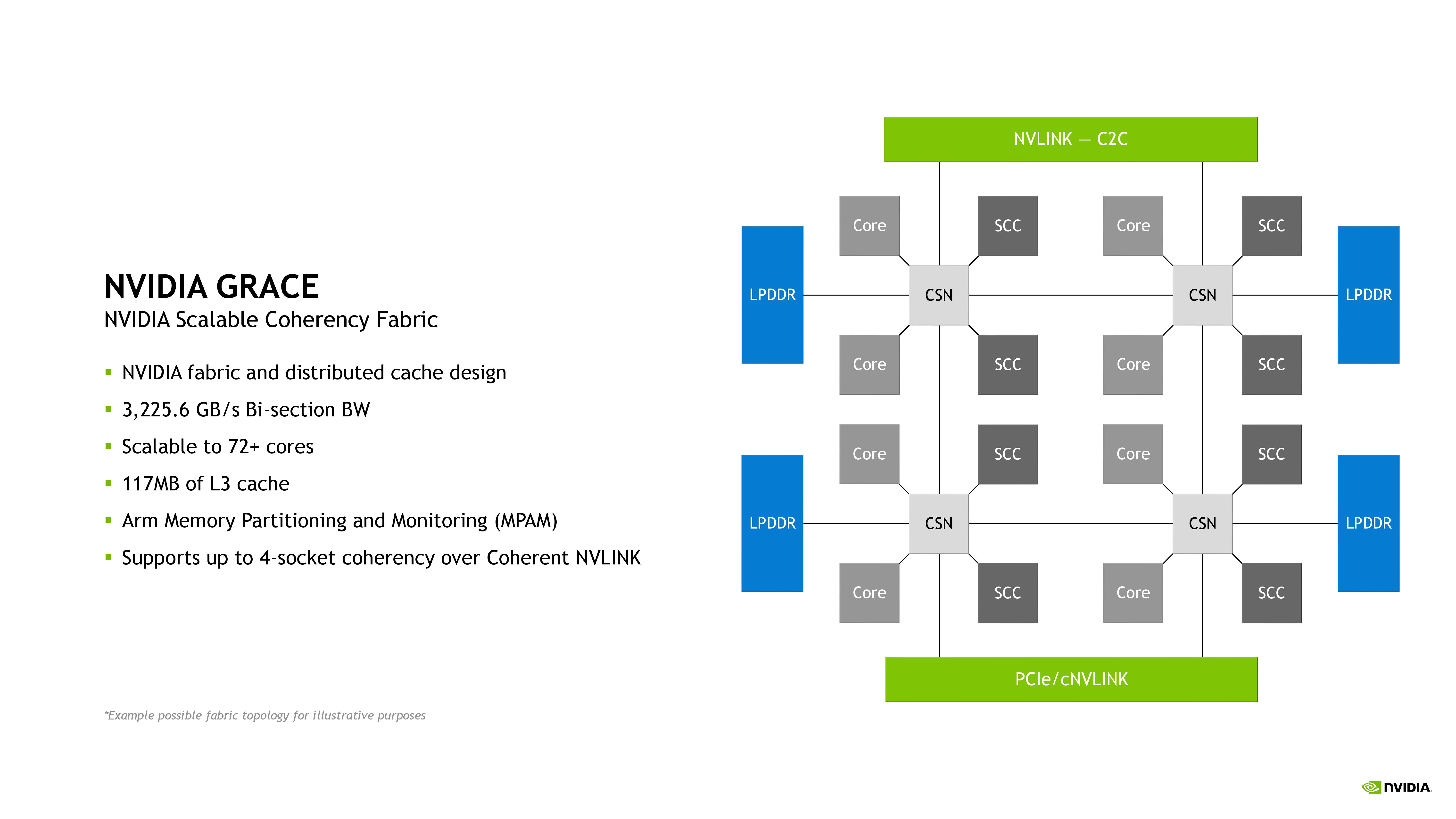
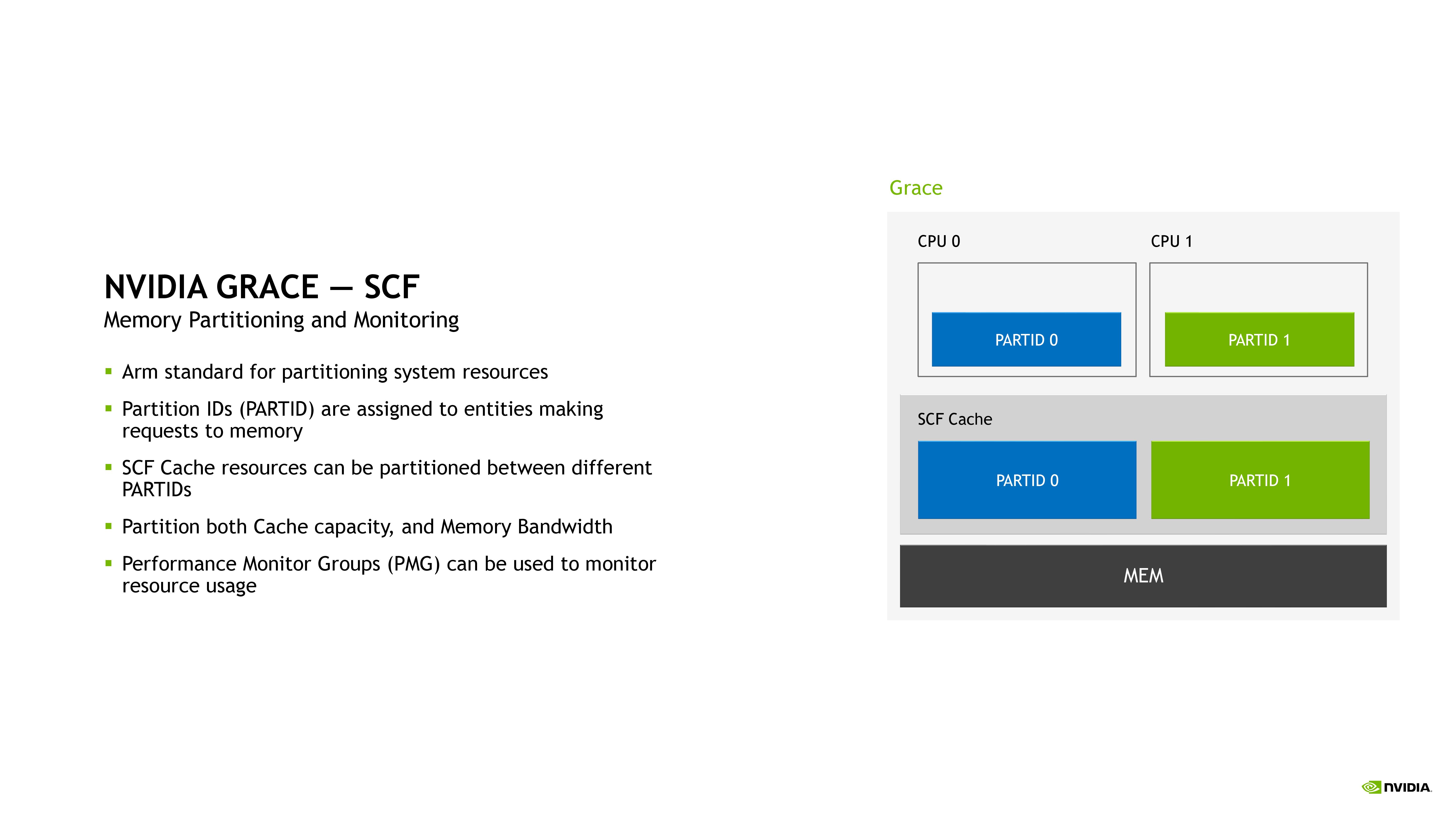
The mesh supports 72+ cores, and each CPU has 117MB of total L3 cache. Nvidia says the first block diagram in the album above is a 'possible topology for illustrative purposes,' and its alignment doesn't entirely agree with the second diagram.
This diagram shows the chip with eight SCF Cache partitions (SCC) that appear to be L3 cache slices (we'll learn more details in the presentation) along with eight CPU units (these appear to be clusters of cores). The SCC and cores are connected to Cache Switch Nodes (CSN) in groups of two, with the CSN then residing on the SCF mesh fabric to provide an interface between the CPU cores and memory to the rest of the chip. SCF also supports coherency across up to four sockets with Coherent NVLink.
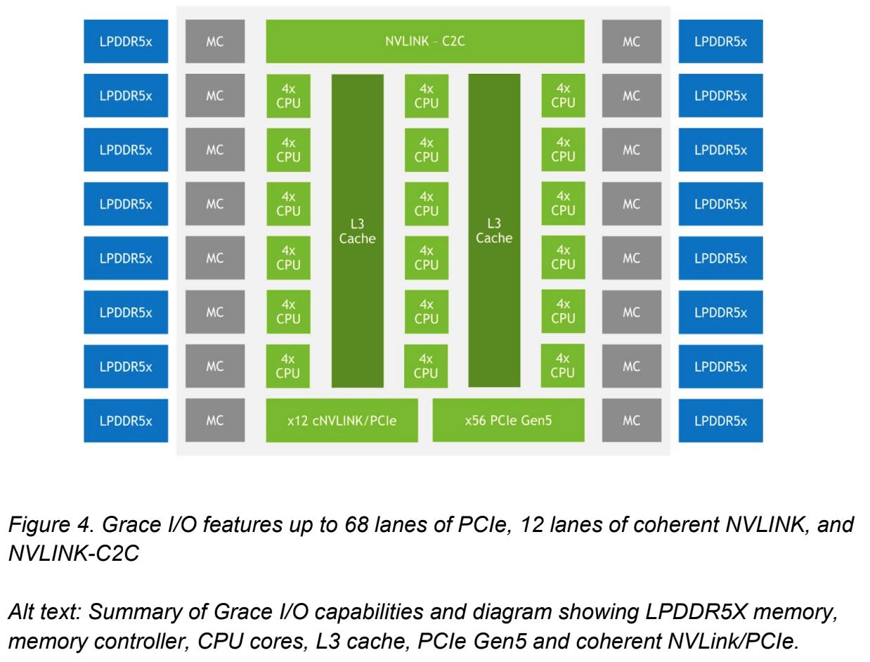
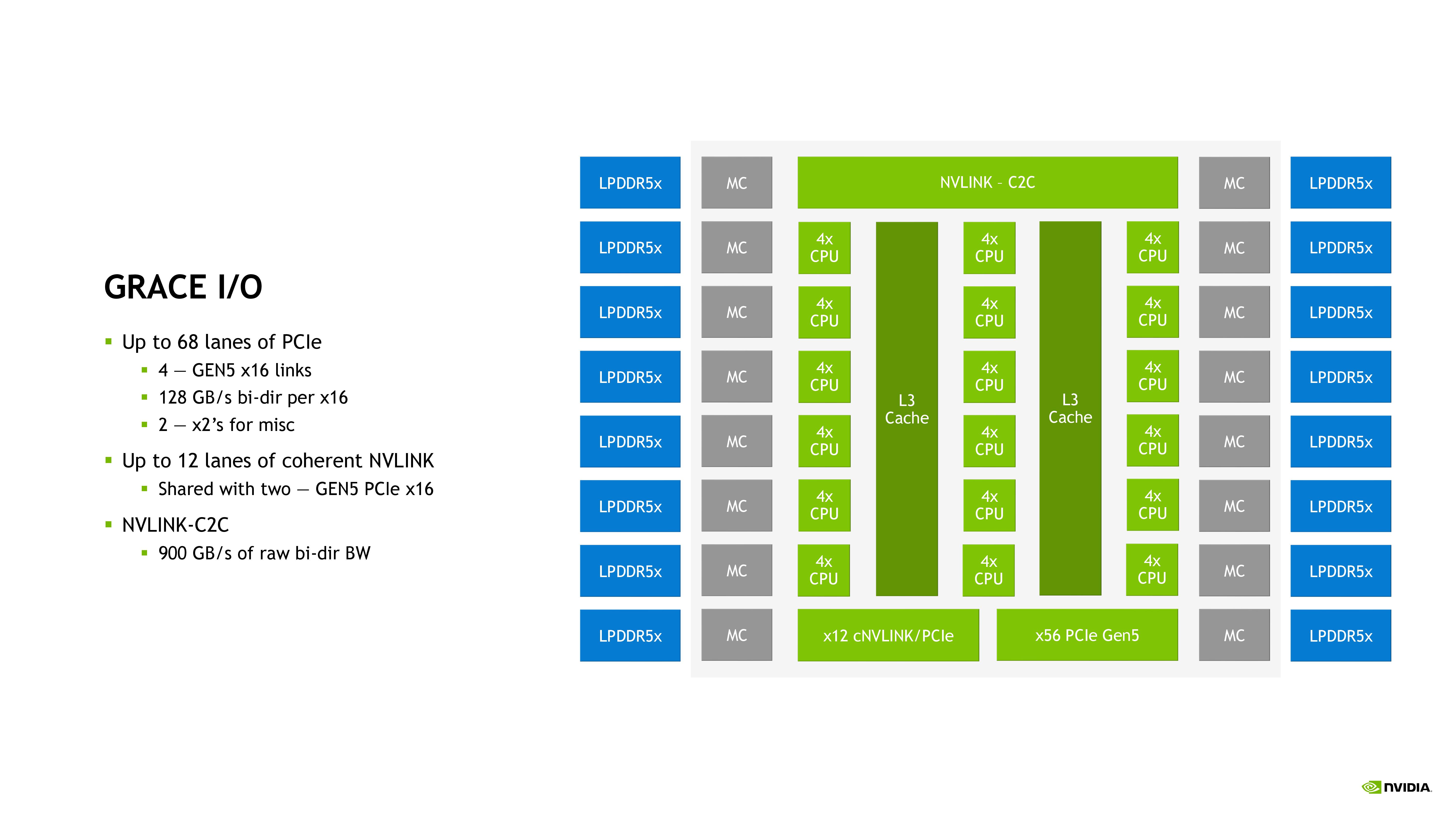
Nvidia also shared this diagram, showing that each Grace CPU supports up to 68 PCIe lanes and up to four PCIe 5.0 x16 connections. Each x16 connection supports up to 128 GB/s of bidirectional throughput (the x16 links can be bifurcated to two x8 links). We also see 16 dual-channel LPDDR5X memory controllers (MC).
However, this diagram is different than the first — it shows the L3 cache as two contiguous blocks connected to quad-core CPU clusters, which makes much more sense than the prior diagram and totals up to 72 cores in the chip. However, we don't see the separate SCF partitions or the CSN nodes from the first diagram, which lends a bit of confusion. We'll suss this out during the presentation and update as necessary.
Nvidia tells us that the Scalable Coherency Fabric (SCF) is its proprietary design, but Arm allows its partners to customize the CMN-700 mesh by adjusting core counts, cache sizes, and using different types of memory, such as DDR5 and HBM, and selecting various interfaces, like PCIe 5.0, CXL, and CCIX. That means it is possible Nvidia uses a highly-customized CMN-700 implementation for the on-die fabric.
Nvidia Grace Hopper Extended GPU Memory
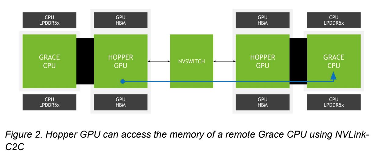
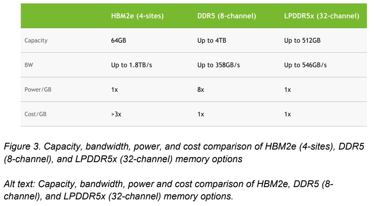
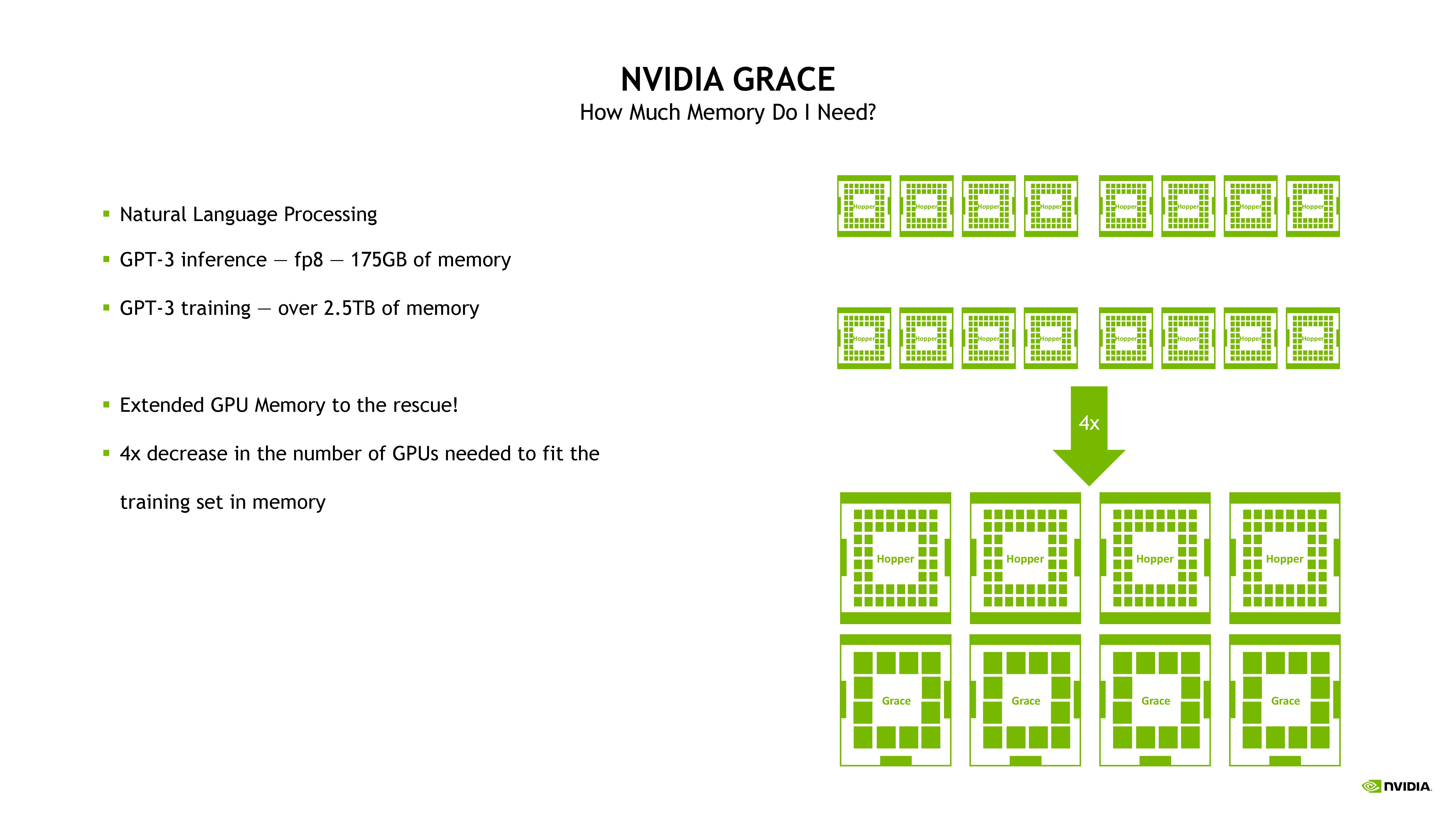
GPUs love memory throughput, so naturally, Nvidia has turned its eye to improving memory throughput not only within the chip but also between the CPU and GPU. The Grace CPU has 16 dual-channel LPDDR5X memory controllers, working out to 32 channels that support up to 512 GB of memory and up to 546 GB/s of throughput. Nvidia says it selected LPDDR5X over HBM2e due to multiple factors, like capacity and cost. Meanwhile, LPDDR5X provides 53% more bandwidth and 1/8th the power-per-GB compared to standard DDR5 memory, making it the better overall choice.
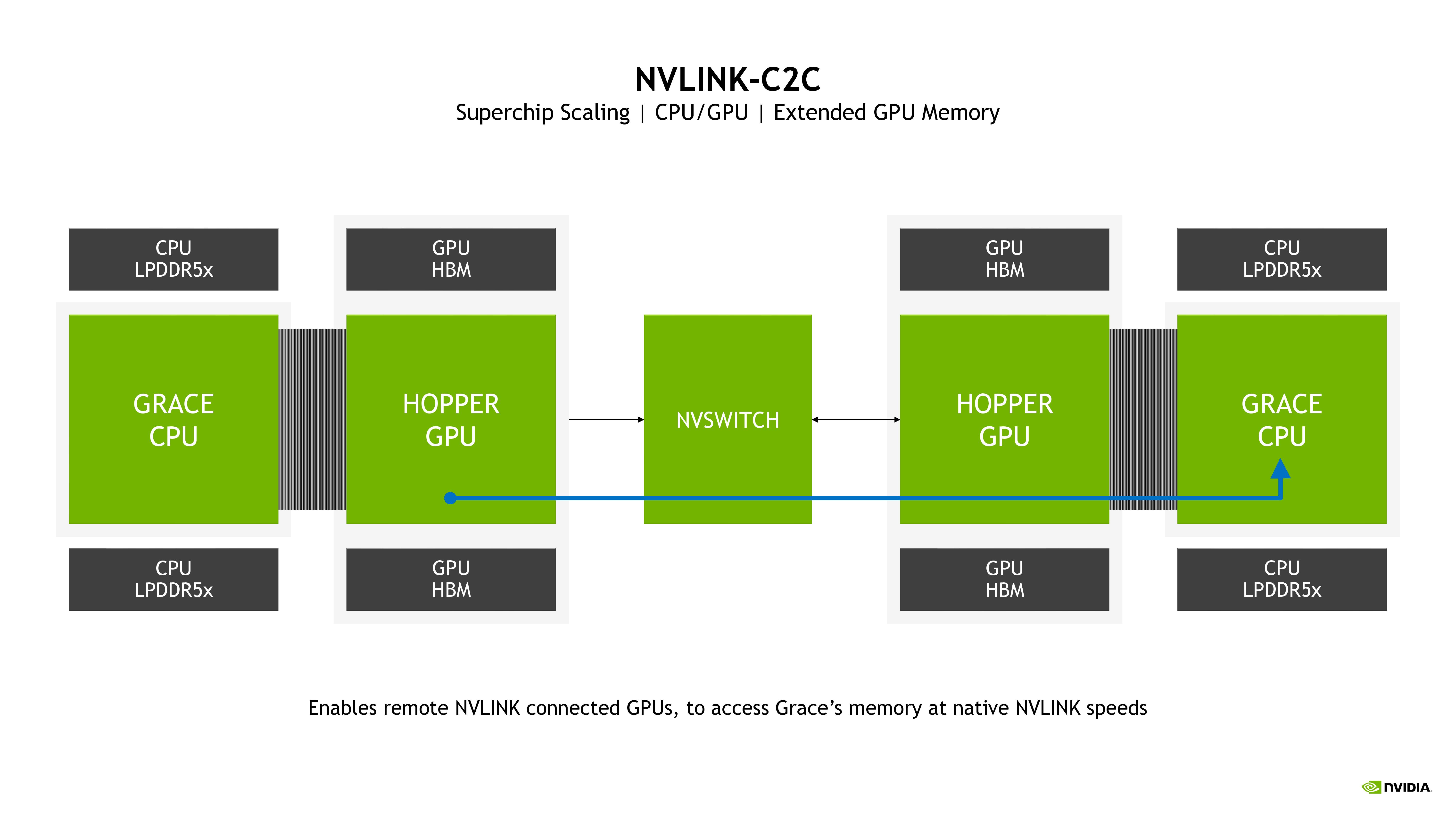
Nvidia is also introducing Extended GPU Memory (EGM), which allows any Hopper GPU on the NVLink network to access the LPDDR5X memory of any Grace CPU on the network, but at native NVLink performance.
Get Tom's Hardware's best news and in-depth reviews, straight to your inbox.
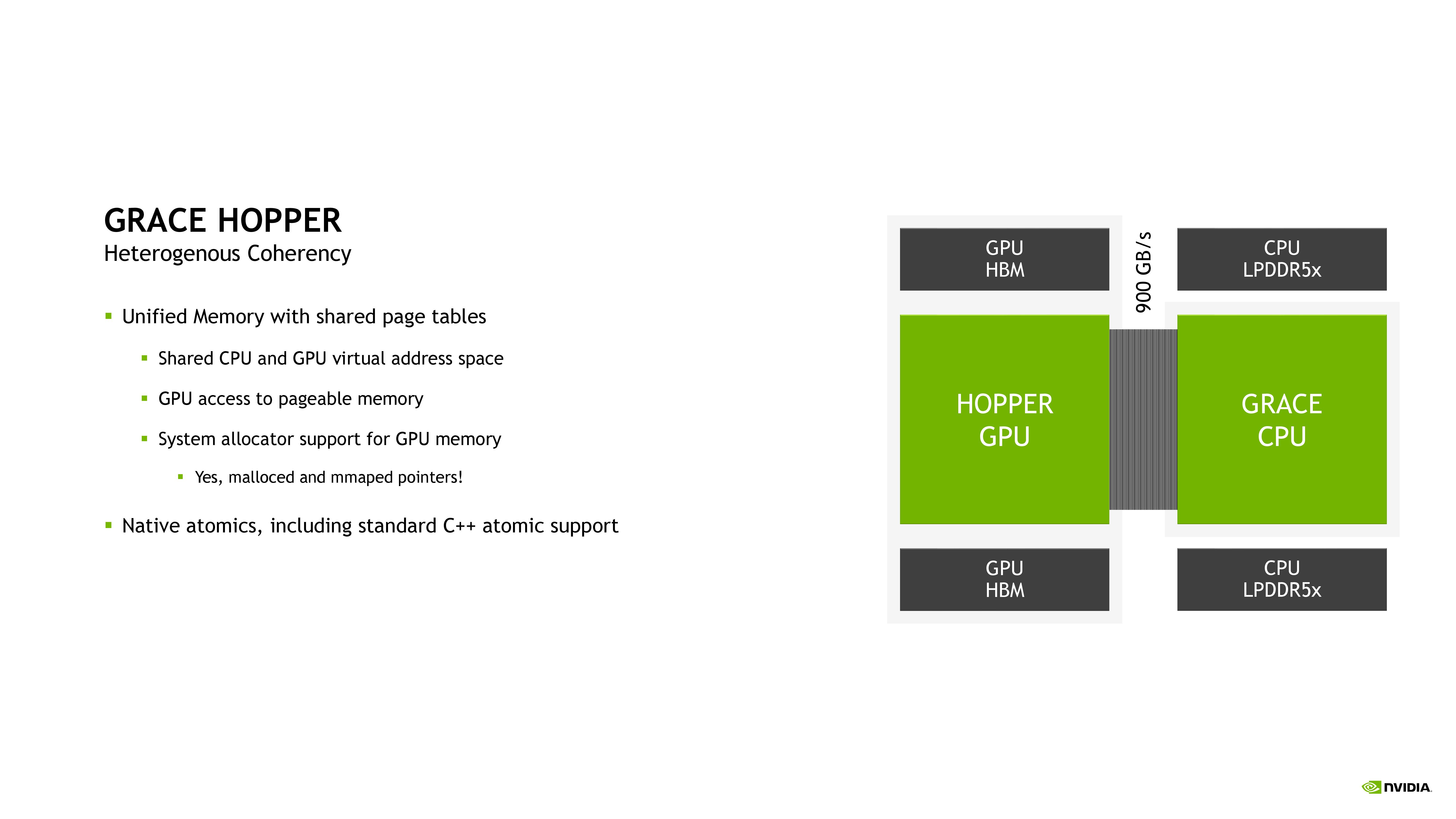
Nvidia's goal is to provide a unified pool of memory that can be shared between the CPU and GPU, thus providing higher performance while simplifying the programming model. The Grace Hopper CPU+GPU chip supports unified memory with shared page tables, meaning the chips can share an address space and page tables with CUDA apps and allows using system allocators to allocate GPU memory. It also supports native atomics between the CPU and GPU.
Nvidia NVLink-C2C
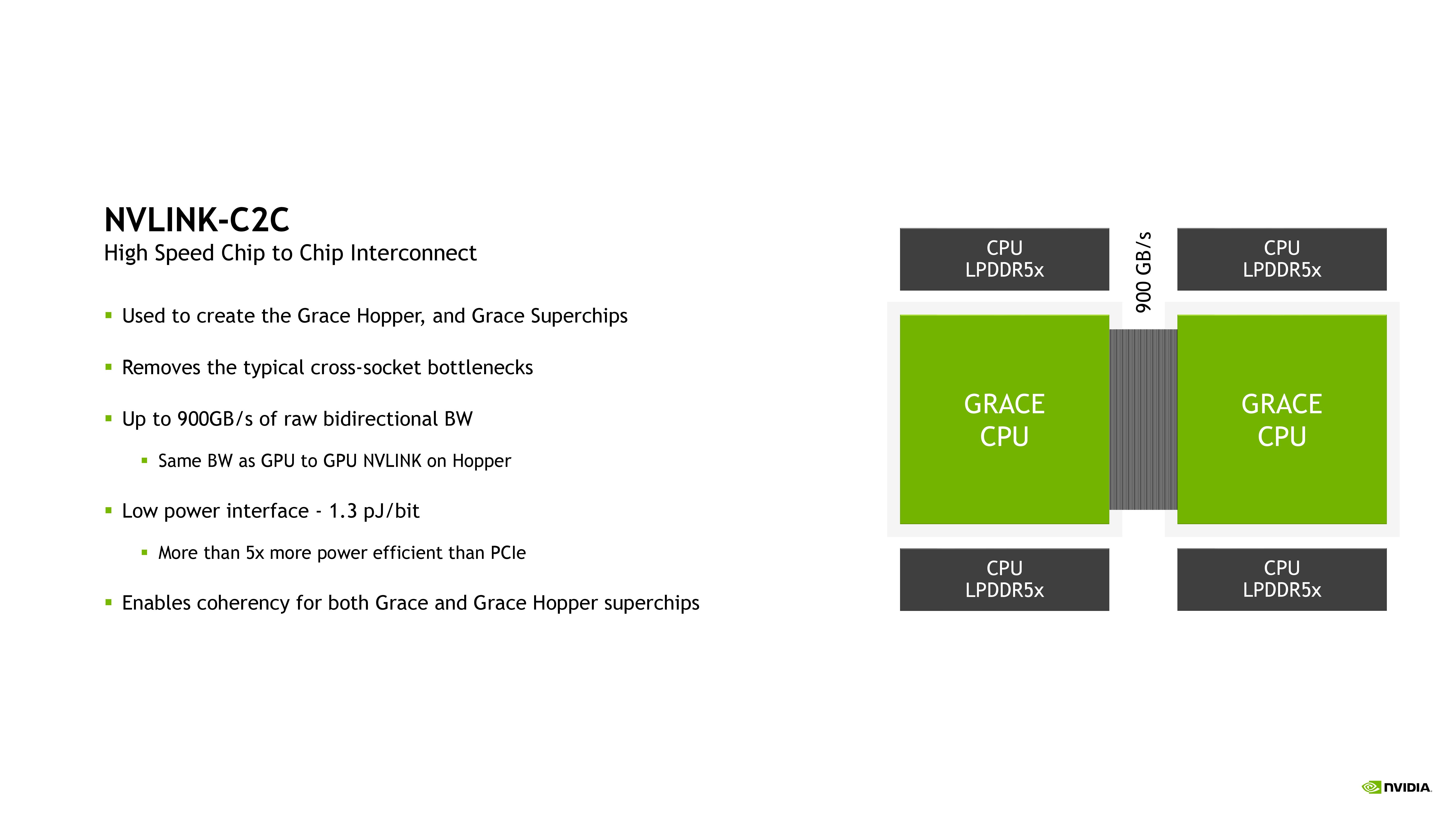
CPU cores are the compute engine, but interconnects are the battleground that will define the future of computing. Moving data consumes more power than actually computing the data, so moving around data faster and more efficiently, or even avoiding data transfers, is a key goal.
Nvidia's Grace CPU, which consists of two CPUs on a single board, and the Grace Hopper Superchip, which consists of one Grace CPU and one Hopper GPU on the same board, are designed to maximize data transfer between the units via a proprietary NVLink Chip-to-Chip (C2C) interconnect and to provide memory coherency to reduce or eliminate data transfers.
| Interconnect | Picojoules per Bit (pJ/b) |
| NVLink-C2C | 1.3 pJ/b |
| UCIe | 0.5 - 0.25 pJ/b |
| Infinity Fabric | ~1.5 pJ/b |
| TSMC CoWoS | 0.56 pJ/b |
| Foveros | Sub-0.3 pJ/b |
| EMIB | 0.3 pJ/b |
| Bunch of Wires (BoW) | 0.7 to 0.5 pJ/b |
| On-die | 0.1 pJ/b |
Nvidia shared new details about its NVLink-C2C interconnect. As a reminder, this is a die-to-die and chip-to-chip interconnect that supports memory coherency, delivering up to 900 GB/s of throughput (7x the bandwidth of a PCIe 5.0 x16 link). This interface uses the NVLink protocol, and Nvidia crafted the interface using its SERDES and LINK design technologies with a focus on energy and area efficiency. The physical C2C interface runs across a standard PCB, so it doesn't use a specialized interposer.
NVLink-C2C also supports industry-standard protocols like CXL and Arm's AMBA Coherent Hub Interface (CHI — key to the Neoverse CMN-700 mesh). It also supports several types of connections ranging from PCB-based interconnects to silicon interposers and wafer-scale implementations.
Power efficiency is a key metric for all data fabrics, and today Nvidia shared that the link consumes 1.3 picojoules per bit (pJ/b) of data transferred. This is 5x the efficiency of the PCIe 5.0 interface, but it is more than twice the power of the UCIe interconnect that will come to market in the future (0.5 to 0.25 pJ/b). Packaging types vary and the C2C link provides Nvidia with a solid blend of performance and efficiency for its specific use case, but as you can see in the table above, more advanced options provide higher levels of power efficiency.
Nvidia Grace CPU Benchmarks
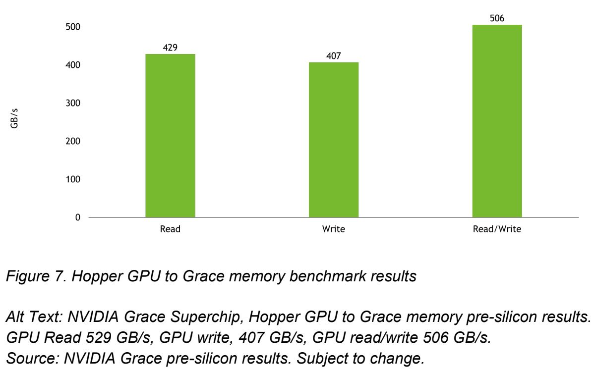
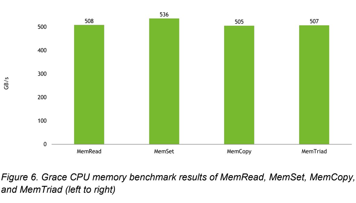
Nvidia shared more performance benchmarks, but as with all vendor-provided performance data, you should take these numbers with a grain of salt. These benchmarks also come with the added caveat that they are conducted pre-silicon, meaning they're emulated projections that haven't been tested with actual silicon yet and are "subject to change." As such, sprinkle some extra salt.
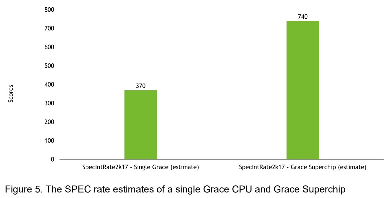
Nvidia's new benchmark here is the score of 370 with a single Grace CPU in the SpecIntRate 2017 benchmark. This places the chips right at the range we would expect — Nvidia has already shared a multi-CPU benchmark, claiming a score of 740 for two Grace CPUs in the SpecIntRate2017 benchmark. Obviously, this suggests a linear scaling improvement with two chips.
AMD's current-gen EPYC Milan chips, the current performance leader in the data center, have posted SPEC results ranging from 382 to 424 apiece, meaning the highest-end x86 chips will still hold the lead. However, Nvidia's solution will have many other advantages, such as power efficiency and a more GPU-friendly design.
Nvidia shared its memory throughput benchmarks, showing that the Grace CPU can provide ~500 GB/s of throughput in CPU memory throughput tests. Nvidia also claims the chip can also push up to 506 GB/s of combined read/write throughput to an attached Hopper GPU, and clocked the CPU to GPU bandwidth at 429 GB/s during read throughput tests, and 407 GB/s with writes.
Grace Hopper is Arm System Ready
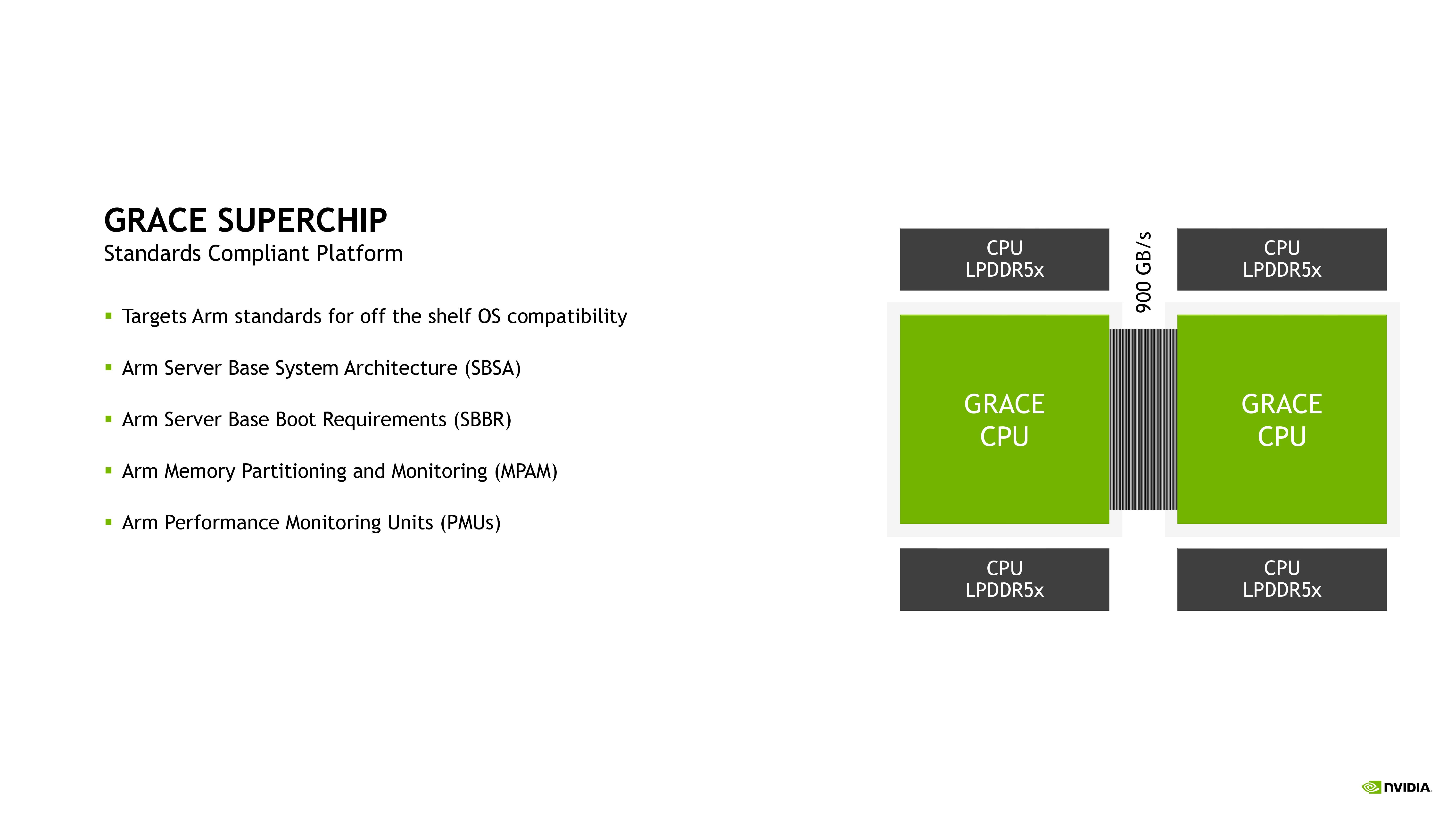
Nvidia also announced that the Grace CPU Superchip will adhere to the necessary requirements to attain System Ready certification. This certification signifies that an Arm chip will 'just work' with operating systems and software, thus easing deployment. Grace will also support virtualization extensions, including nested virtualization and S-EL2 support. Nvidia also lists support for the following:
- RAS v1.1 Generic Interrupt Controller (GIC) v4.1
- Memory Partitioning and Monitoring (MPAM)
- System Memory Management Unit (SMMU) v3.1
- Arm Server Base System Architecture (SBSA) to enable standards-compliant hardware and software interfaces. In addition, to enable standard boot flows on Grace CPU-based systems, Grace CPU has been designed to support Arm Server Base Boot Requirements (SBBR).
- For cache and bandwidth partitioning, as well as bandwidth monitoring, Grace CPU also supports Arm Memory Partitioning and Monitoring (MPAM). Grace CPU also includes Arm Performance Monitoring Units, allowing for the performance monitoring of the CPU cores as well as other subsystems in the system-on-a-chip (SoC) architecture. This enables standard tools, such as Linux perf, to be used for performance investigations.
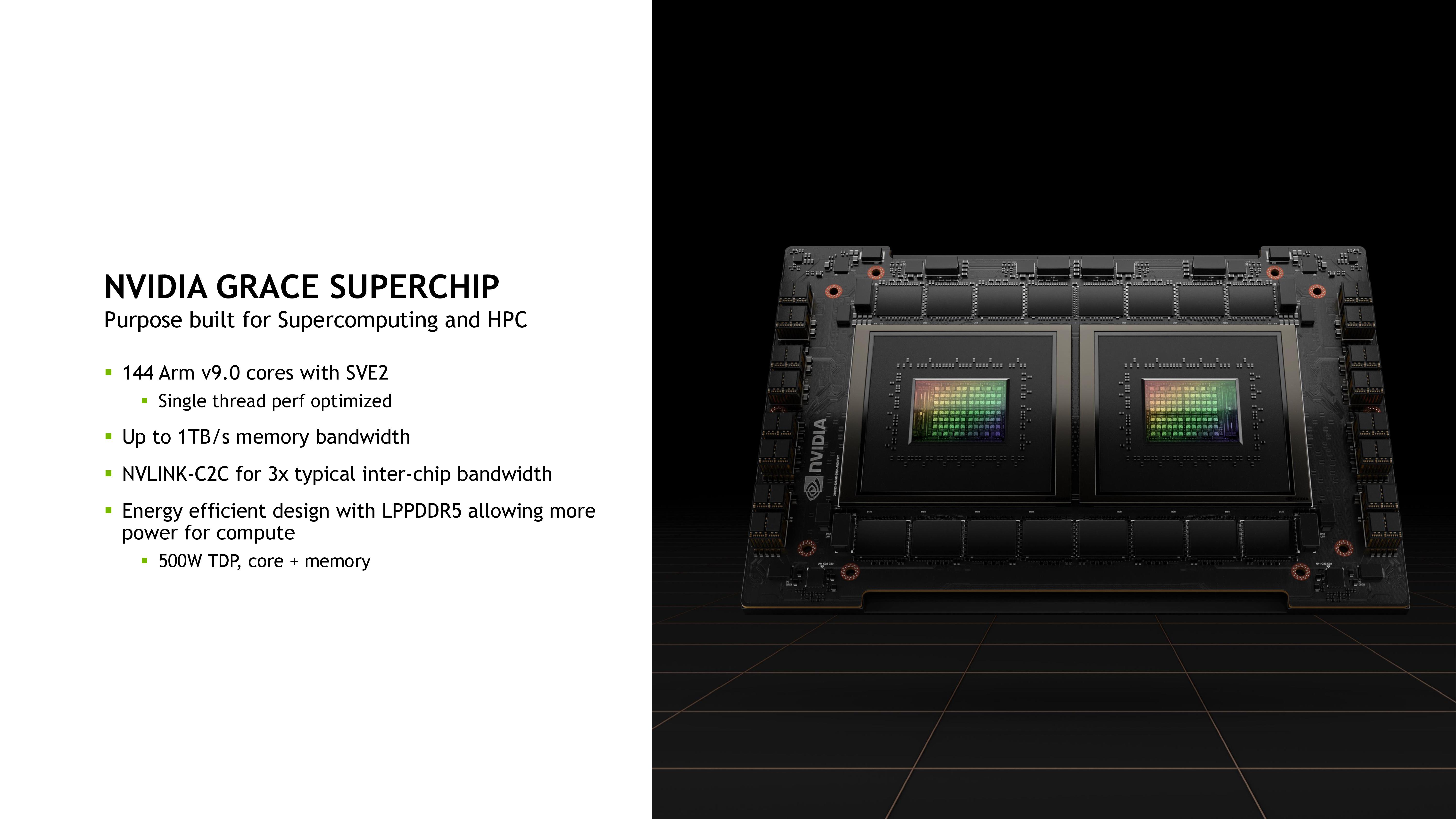
Nvidia's Grace CPU and Grace Hopper Superchip are on track for release in early 2023, with the Hopper variant geared for AI training, inference, and HPC, while the dual-CPU Grace systems are designed for HPC and cloud computing workloads.

Paul Alcorn is the Editor-in-Chief for Tom's Hardware US. He also writes news and reviews on CPUs, storage, and enterprise hardware.
-
bit_user Thanks for the coverage @PaulAlcorn . I especially appreciated the interconnect comparison table!Reply
I'm definitely looking forward to any coverage of Hot Chips you can provide!