Intel Details Its Bitcoin-Mining 'Bonanza Mine' Chips and 3,600-Watt Miner
Intel's 3,600-watt Bitcoin-mining powerhouse
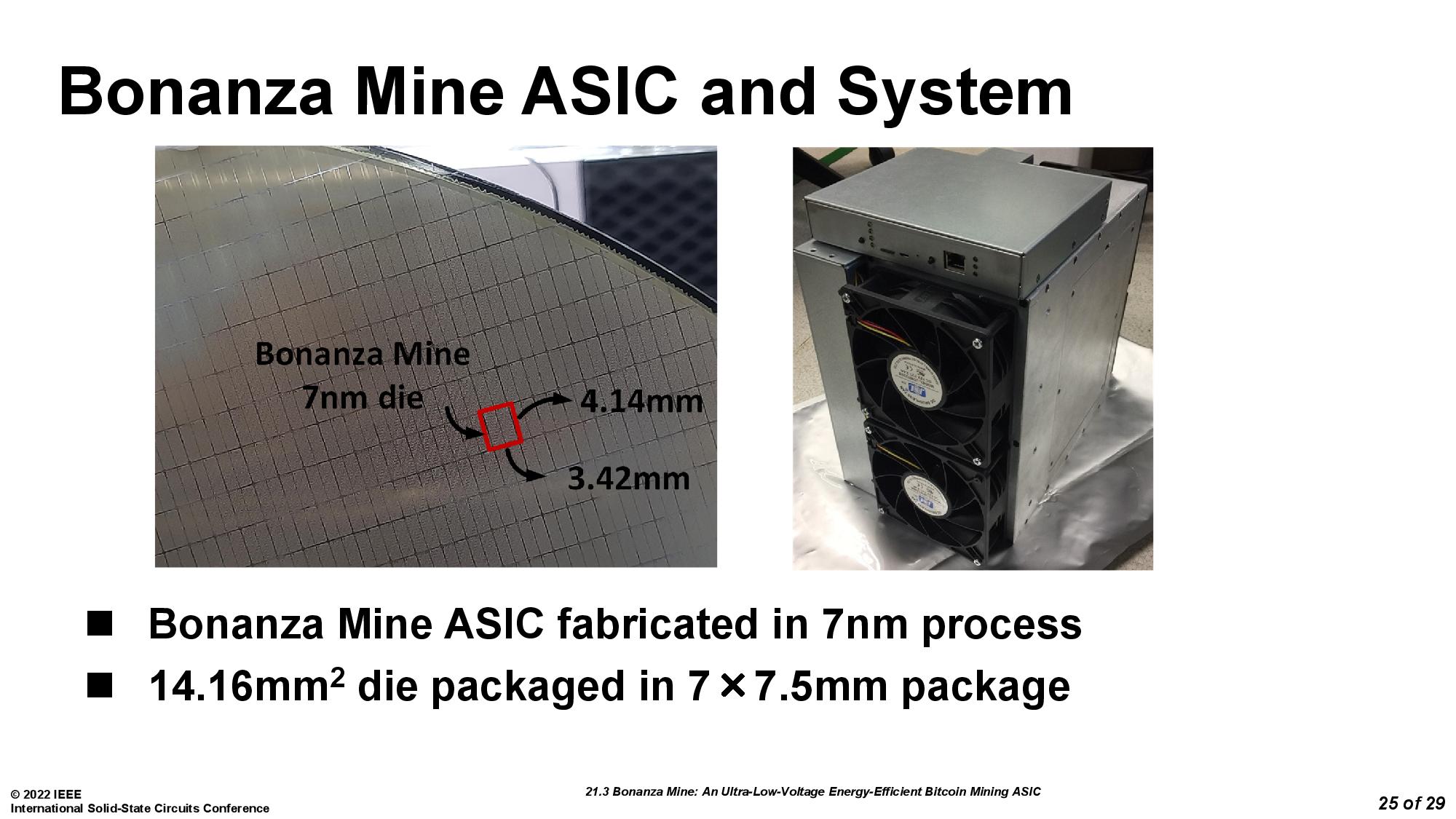
At ISSCC 2022, Intel shared the deep-dive details of its new Bitcoin-mining Bonanza Mine ASICs and outlined how it melds 300 of these tiny power-efficient chips into a powerful 3,600W miner that delivers up to 40 THash/s of performance. [EDIT: We have since found the specifications and pricing for the newer model that is shipping to customers, which you can read about here.]
We first discovered Intel's Bonanza Mine ASICs in a listing for a presentation at the ISSCC 2022 conference, and the information below comes from the presentations at the event. This material covers the first generation of Intel's mining chips, known as BZM1, but the company has already moved on to its second-gen 'Bonanza Mine' ASIC, known as BZM2, that it is now making available to customers to challenge the likes of Bitmain and MicroBT.
After news of the company's efforts came to light, Intel finally officially acknowledged its blockchain/Bitcoin silicon program, divulging that it already has several large customers for the second-gen chips. That includes BLOCK (helmed by CEO Jack Dorsey of Twitter fame), Argo Blockchain, and GRIID Infrastructure.
Intel hasn't shared details of the second-gen chips and systems yet, but we do know they are derivatives of the BZM1 ASICs shown below.
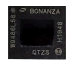
Here we can see the BZM1 chip in its rather small 7 x 7.5mm exposed-die FCLGA package (132 balls). As you'll see below, 300 of these chips power the system.
Each chip die measures 4.14 x 3.42mm, for a total of 14.16mm^2 of silicon, so these are comparatively small slivers of silicon. The smaller die size improves yield and maximizes wafer area usage (up to 4,000 die per wafer), thus helping maximize production capacity (though it does require more wafer dicing/packaging capacity). Intel says these are 7nm ASICs, but doesn't specify if that is its own 'Intel 7,' the original 7nm before it renamed the process node to 'Intel 4,' or TSMC's 7nm process.
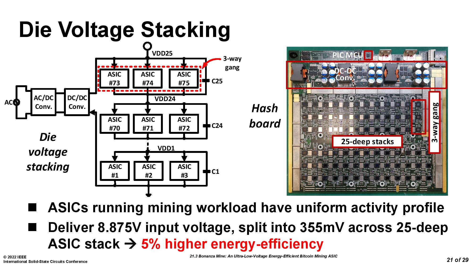
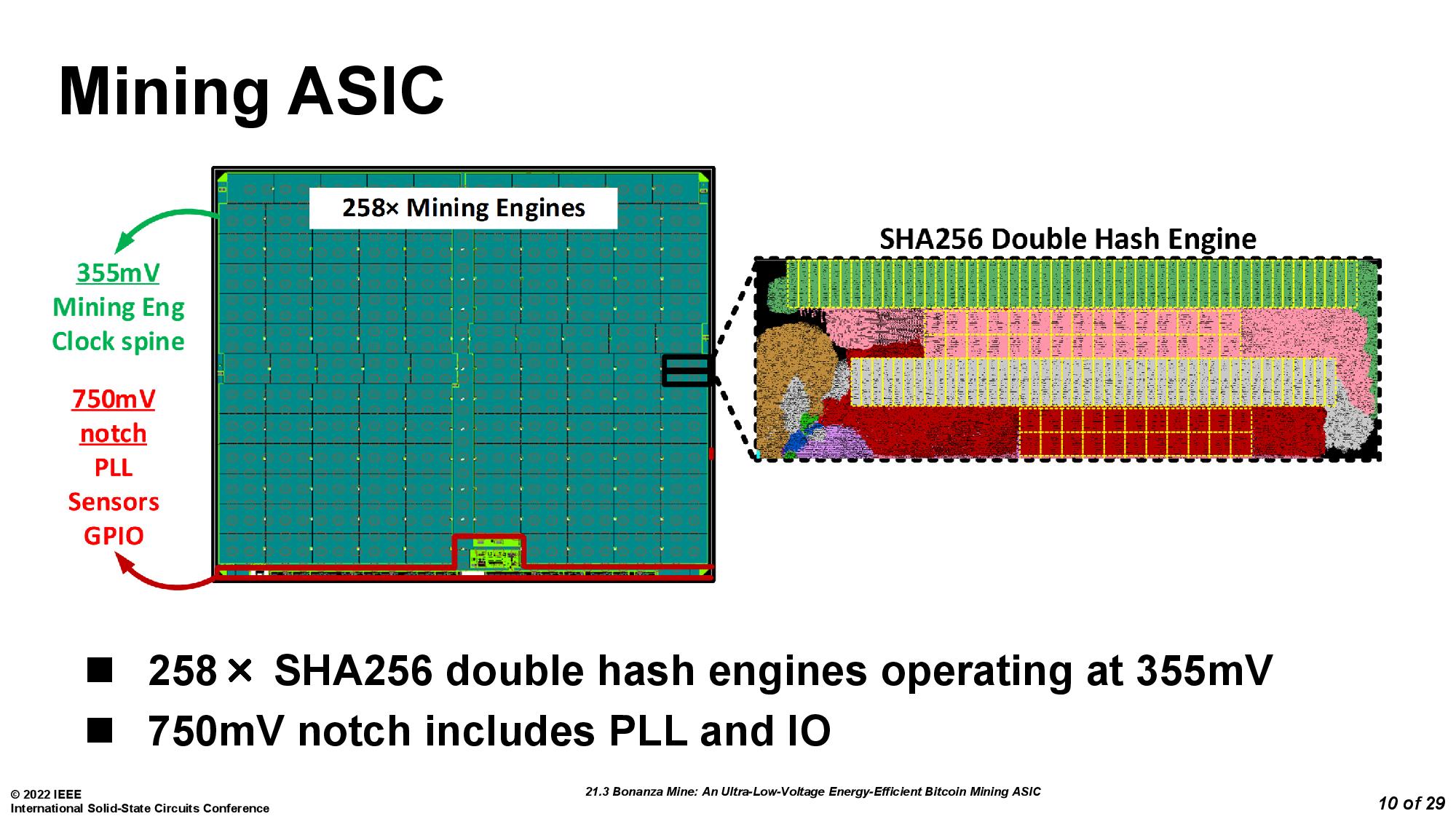
Each Bonanza Mine ASIC has 258 mining engines, and each engine computes parallel SHA256 double hashes. These engines comprise 90% of the die area and operate at what Intel characterizes as an 'ultra-low' voltage of 355mV.
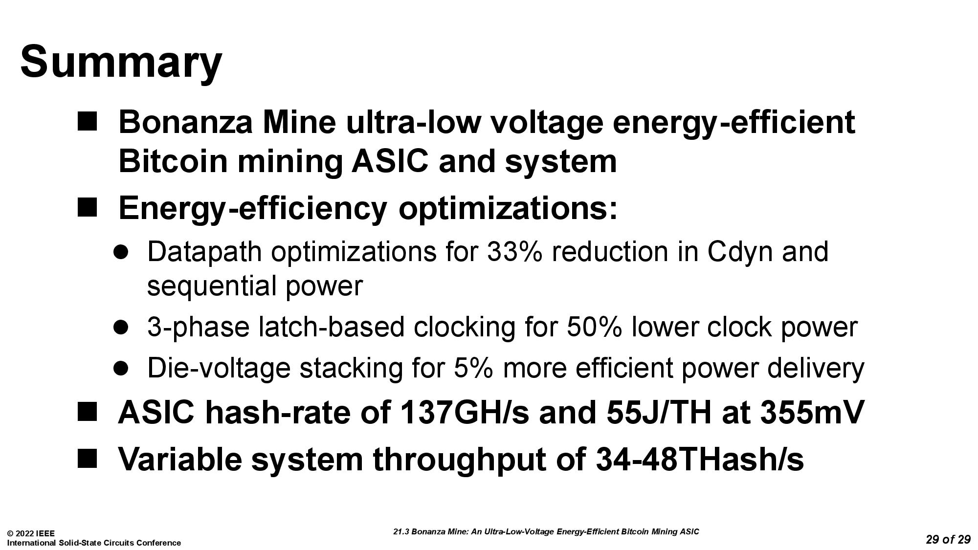
Each ASIC operates at 1.35 to 1.6 GHz at 75C, consuming an average of 7.5W apiece while hitting up to 137 Ghash/s. That works out to 55 J/THash/s at 355mV.
Zooming out to the 300 chips in the system, there's a total of 4,248mm^2 of silicon that delivers up to 40TH/s at 3600W of power consumption. It's clear that Intel will need to be far more competitive against Bitmain and MicroBT's existing miners. For instance, Bitmain's Antmienr S19j Pro 104T does 104 THash/s at 3,068W, while the newest model, the S19j XP, does 140 THash/s at 3010W. Again, these are Intel's first-gen Bonanza Mine chips, but its new contracts are for the second-gen 'BZM2' models that remain shrouded in mystery.
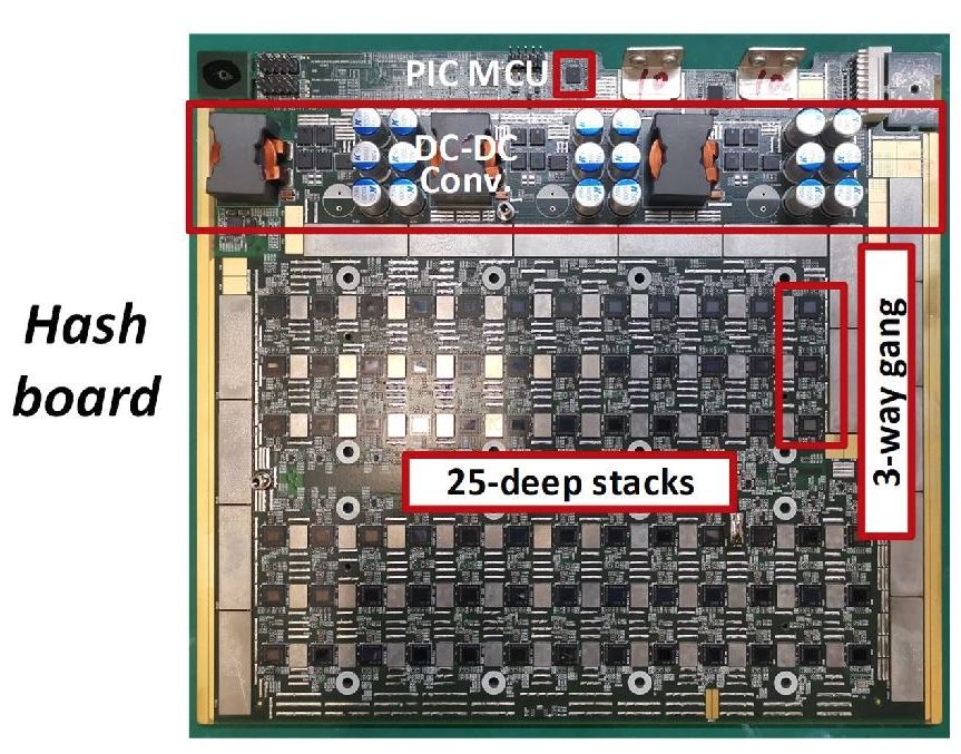
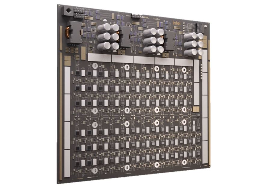
Intel solders on 75 Bonanza Mine ASICs per hash board, arranged in 25-deep voltage stacks with ganged stack-voltages. The hash board also houses a microcontroller that manages power-on and thermal/stack-voltage monitoring. A 10MB/s UART serial link shuffles data between the chips and the control unit that sits atop the full system.
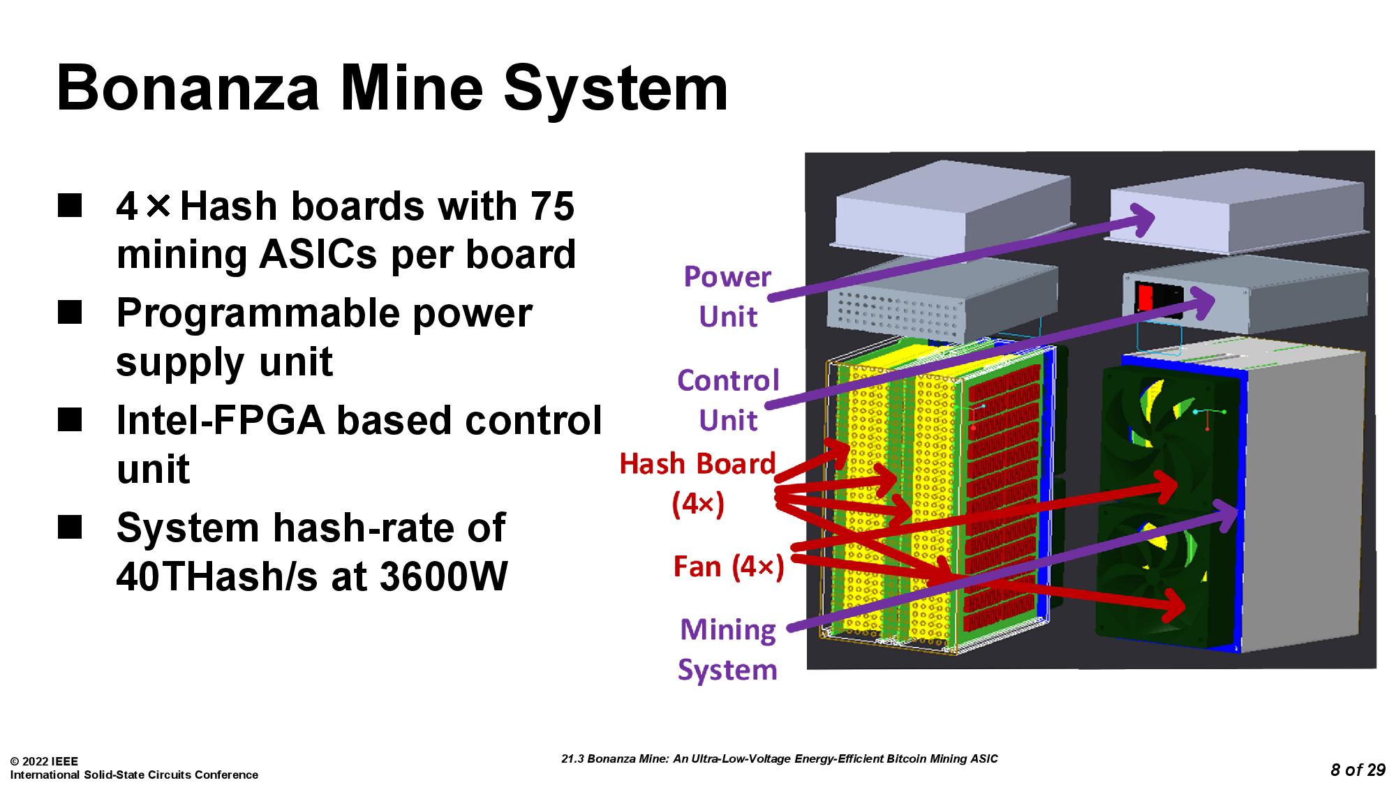
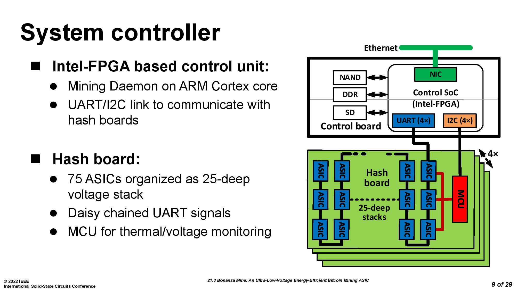
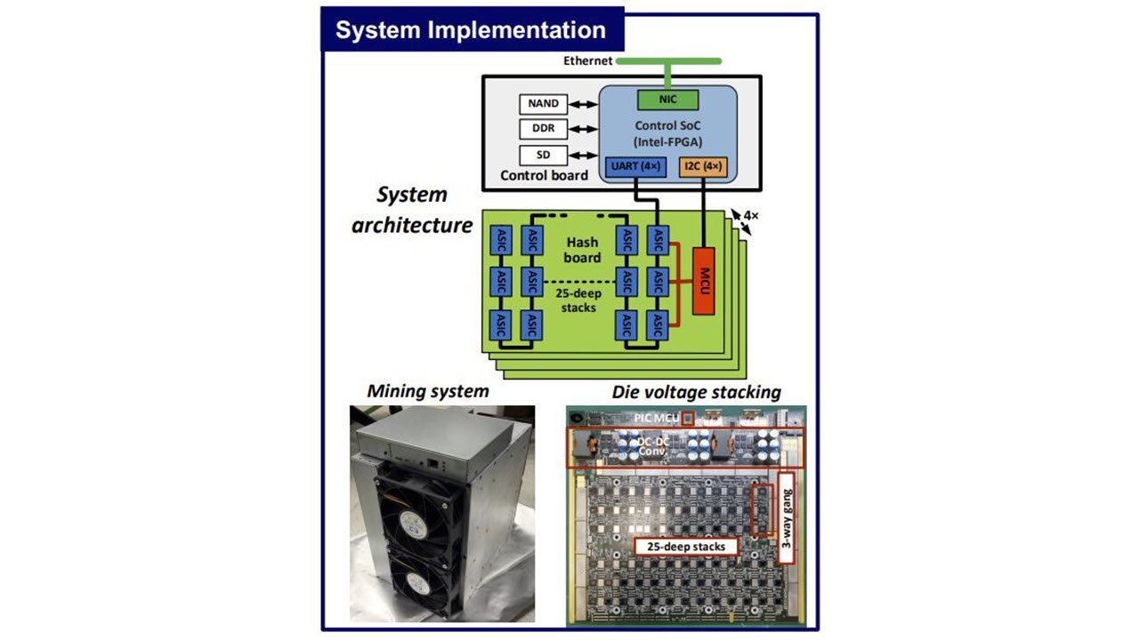
Here we can see both the block diagram and images of the full system. Four hash boards are placed vertically into a single unit with four fans that keep the system cool.
The control unit sits atop the device, housing an Intel-FPGA-based system controller and an Arm Cortex core that runs the mining daemon and distributes the work among the 300 chips. The ARM core also adjusts the on-die PLLs to control chip frequencies and verify the ASICs' hash results. As you would expect, the unit also has an Ethernet connection to communicate with a larger mining pool. The system also has a programmable power supply.
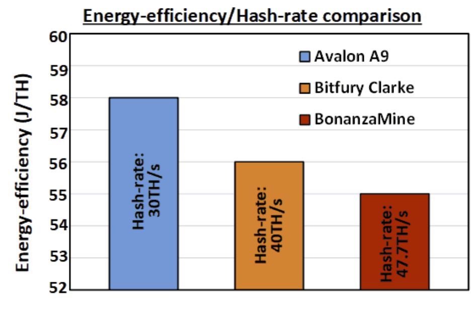
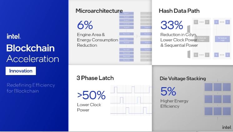
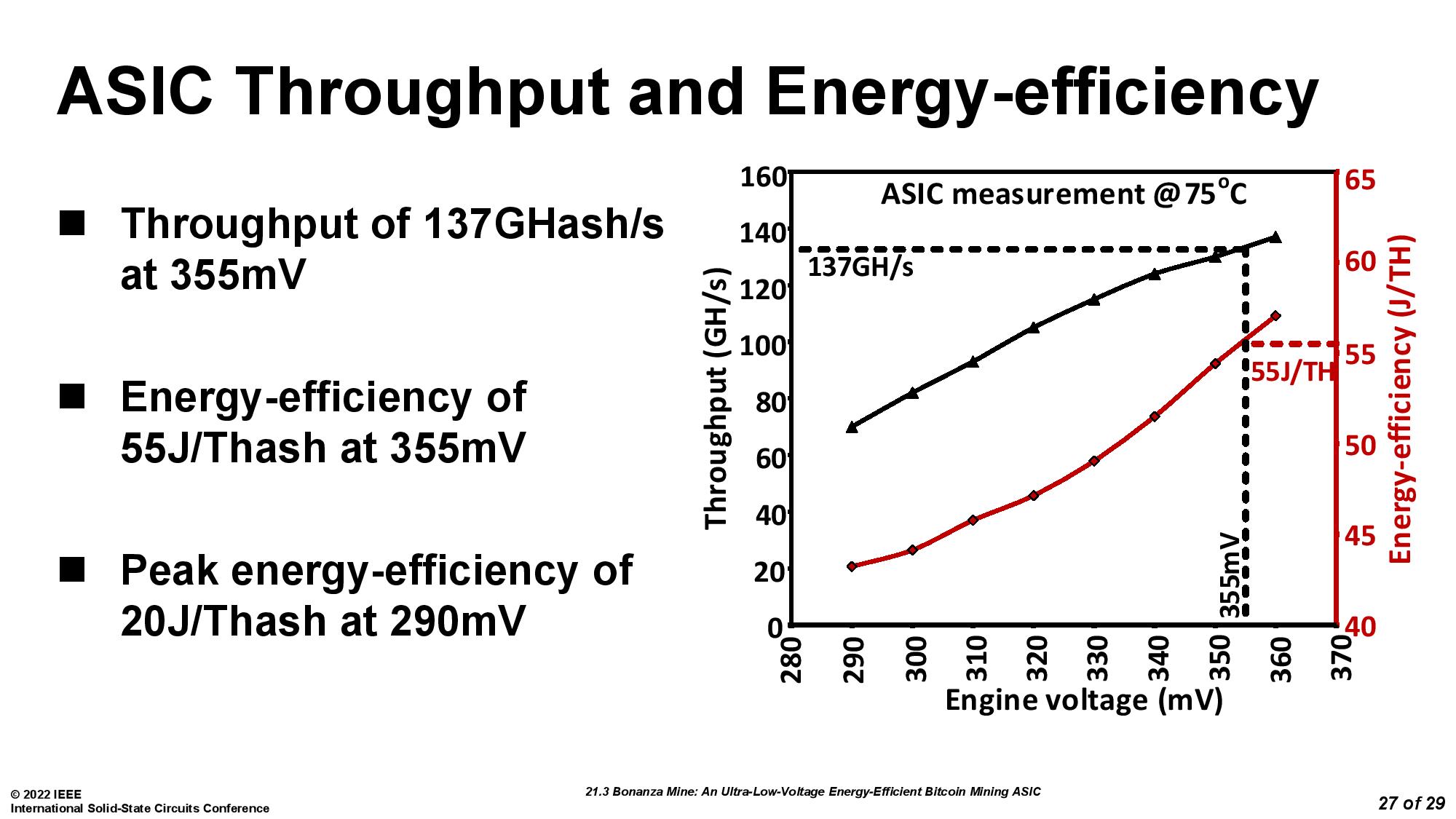
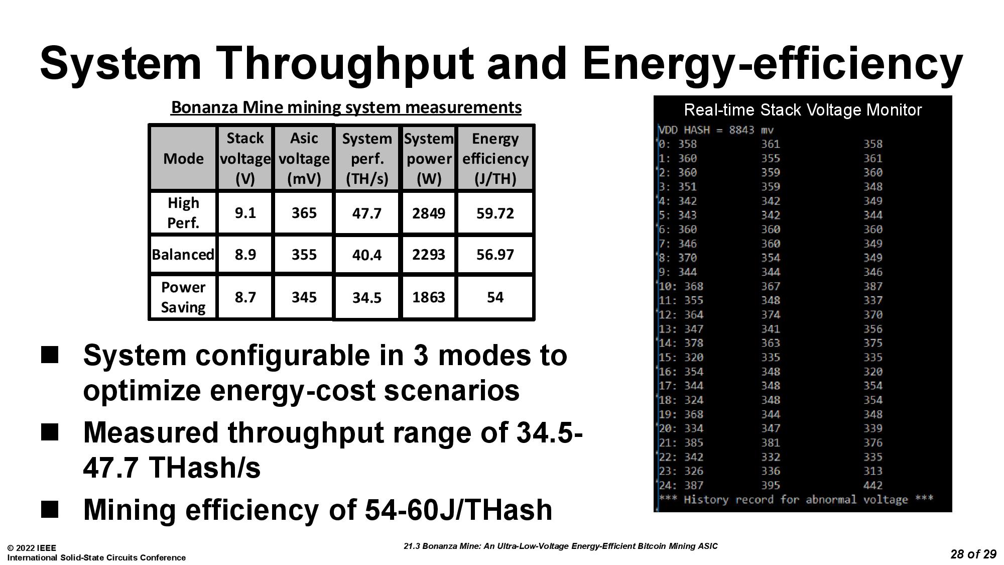
As shown above, the system can operate in different power/thermal profiles, like Power-Saving, Balanced, and High-Performance, to tailor the usage profile, thus yielding anywhere from 54 to 60 J/THash.
Intel built the system described above from the first-gen Bonanza Mine chips. However, Intel's second-gen chips can obviously be used in several configurations: GRIID's supply agreement with Intel has plenty of redactions to protect sensitive information, but it also heavily references Intel's Reference Design Materials. These are a series of documents that customers use as guidance when integrating the Bonanza Mine chips into their own custom systems.
This implies that Intel will supply the silicon to some of its customers, who will then create their own systems. This also meshes well with Jack Dorsey's plans for BLOCK, which he says will create a "bitcoin mining system based on custom silicon and open source for individuals and businesses worldwide." Of course, Intel could also manufacture complete mining systems and bring them to market through partners, but we'll have to wait to learn more about its go-to-market strategy.
Intel's first-gen Bonanza Mine chip sets a promising tone for its second-gen Bonanza Mine chips that are already working their way out to customers. However, there are still plenty of unknowns about the technical details of the second-gen chips, like performance, efficiency, pricing, power consumption, the process node, foundry used, and so on. We also don't know Intel's plans for its future roadmap.
Intel has a question and answer session scheduled at ISSCC for later in the week, and we'll follow up with more information after.
Update 2/20/2020: Added details about Bitmain performance.
Get Tom's Hardware's best news and in-depth reviews, straight to your inbox.

Paul Alcorn is the Editor-in-Chief for Tom's Hardware US. He also writes news and reviews on CPUs, storage, and enterprise hardware.
-
bluvg "Intel says these are 7nm ASICs, but doesn't specify if that is its own 'Intel 7,' the original 7nm before it renamed the process node to 'Intel 4,' or TSMC's 7nm process."Reply
Please, don't continue using "nm" as an actual measure. It hasn't been for a long time; it's now an extrapolation. Transistor density is a much more useful metric for comparison. Intel renamed its current process to Intel 7 because it is of analogous density to TSMS's N7 (note TSMC also doesn't label it "7nm"). -
Kenneth Harden Please, for the love of all that is holy, let 'something else' (besides gaming GPUs) be the smart choice for mining and pull the rug out from under that market. Honestly, if this keeps up for too much longer it is going to start doing real damage to the PC gaming industry.Reply
I am thankful I have a 'pre crazy times' 2080 that is serving me well, but I constantly worry about what happens if it dies. Well I do have an old 760 sitting in a box! -
getoutmining Are you sure about those specs? 40TH at 3600W is poor. New Bitmain is 140TH at 3000W.Reply -
Foulbelly Replygetoutmining said:Are you sure about those specs? 40TH at 3600W is poor. New Bitmain is 140TH at 3000W.
I was thinking the same thing.
Bitmain's current flagship antminer s19pro is actually 110th/s @3250w. Canaan flagship Avalon 1246 runs 90th/s @ 3400w.
Either way, the best offerings from Bitmain (s19p) and Canaan (a1246) absolutely blow the doors off of Intel's latest offering. Not sure what I'm missing here.... Intel has to increase their efficiency by 60% or more to come close to matching current iterations. -
Exploding PSU ReplyKenneth Harden said:Please, for the love of all that is holy, let 'something else' (besides gaming GPUs) be the smart choice for mining and pull the rug out from under that market. Honestly, if this keeps up for too much longer it is going to start doing real damage to the PC gaming industry.
I am thankful I have a 'pre crazy times' 2080 that is serving me well, but I constantly worry about what happens if it dies. Well I do have an old 760 sitting in a box!
I hear you. If my Vega 56 dies my 970 would need to come out of retirement and start pumping frames again