Micron Outs 3D NAND Technical Details, 3D SSDs Landing In June
When Micron officially announced first generation 3D NAND flash technology, the company claimed this would lead to 3.5 TB gum stick-sized SSDs and more than 10 TB standard 2.5-inch SSDs. In our latest briefing, we learned more about the technology that will bring these products to reality.
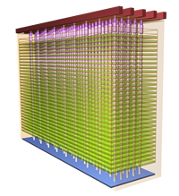
Most flash sold today is planar (2D), like a single story home. The technology progressed by fitting more bits in the same amount of space. To do so, the size and the distance between each bit needed to shrink. 3D technology increases density by building layers of cells vertically, like a skyscraper. The vertical skyscraper holds more data in the same footprint than a single story structure.
The Structure
Micron's first generation 3D flash technology uses 32 layers to build a single die. In multi-level cell (MLC) mode, the die density comes to 256 Gbit. Competing technology shipping today needs 48 layers to achieve the same density. In 3-bit per cell mode (TLC), the same die holds 384 Gbit of data. The new cells double the bit density compared to Micron's 16nm planar NAND. The block sizes increase to 16 MB for MLC and 24 MB for TLC modes.
Article continues belowThe increased density comes, in part, from Micron's CMOS Under the Array technology. In planar NAND, the logic cells that control the flash makes up as much as 20% of the overall size. With the logic control tucked under the storage portion of the die, like a basement or parking garage, more storage capacity can fit in the same footprint.
The CMOS also handles special functions like FortisFlash, used to deliver advanced ECC solutions on die, and SLC areas used to increase write performance.
The new storage structure uses floating gate technology. Micron claimed this combats charge loss better than charge trap technology used by its competitors. With less loss, Micron's 3D flash will require less error correct technology that consumes more power over time. In theory, floating gates will also allow Micron to be much more aggressive with the vertical stack from generation to generation. SK Hynix attempted to build 3D NAND flash with floating gates but eventually scrapped the project to build on charge trap technology. It's our understanding that floating gates are much more difficult to build vertically, but at the same time, it's the technology Micron and Intel mastered long ago.
The new 3D flash moves to Open NAND Flash Interface (ONFi) 4.0, a specification built and maintained by Intel, Micron, Phison, SanDisk, SK Hynix and others to build a common interface for flash. The fourth revision increases performance up to 800 MT/s with a quad plane path and reduced power to just 1.2 volts.
Get Tom's Hardware's best news and in-depth reviews, straight to your inbox.
Endurance is often a subject that NAND flash manufacturers try to avoid, but not this time. Paired with Low Density Parity Check (LDPC) error correction technology, MLC 3D flash from Micron can deliver up to 30,000 program / erase (P/E) cycles. The high endurance also enables TLC in the enterprise (eTLC).
Benefits
The change in power means Micron's new 3D 32-layer flash can move up to 30% more data with the same amount of power used today with planar NAND. This will increase notebook battery life and reduce datacenter power consumption.
The new density will double die capacity in end products, effectively making 256 GB models the new 128 GB drives of today. Without any special configurations, 2 TB SSDs will be possible at the time of retail availability and shouldn't have a large price premium over existing 1 TB SSDs sold today. The increase in endurance will also take us back to a time when it was an afterthought and rarely discussed outside of the enterprise market.
Retail Availability
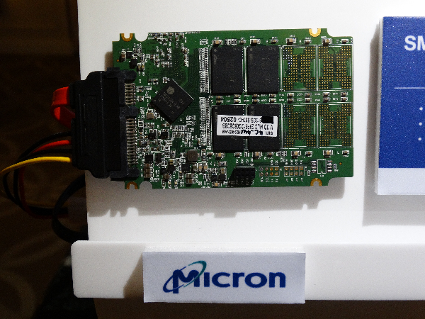
At CES, we saw client SSDs in the R&D stage armed with Micron 3D MLC. Micron told us the first retail products should arrive in June, around the Computex time frame. Client SSDs paired with 3D MLC should arrive first with TLC products soon after. Eventually, TLC will dominate the client market -- even high-performance PCIe based models.
Micron has worked closely with Silicon Motion, Inc. on a client solution, and with PMC Sierra for an enterprise product. The time frame lines up with what we've heard from other companies eager to tap into the vertical pipeline.
We pressed Micron about a potential 3D TLC / 3D XPoint pairing wherein XPoint acts as a large, high performance buffer for slower TLC NAND. we were told, "We can't talk about that, but it would make a very good cache or buffer."
The combination is obvious but would require an advanced controller and programming. We will have to wait on a XPoint update to learn more.

Chris Ramseyer was a senior contributing editor for Tom's Hardware. He tested and reviewed consumer storage.
-
tsnor ReplyWhat connection interface will this use?
Open NAND Flash Interface (ONFi) 4.0 is how you talk to the flash. The controller that talks to the flash would then choose an interface back to the host system like NDMe or SAS or SATA. -
uglyduckling81 Shouldn't this article really say Micron catch up to Samsung's current gen hardware rather than say anything about next gen? 3D NAND has been in use in Sammy SSD's for what?... A year or more right?Reply -
aldaia ReplyShouldn't this article really say Micron catch up to Samsung's current gen hardware rather than say anything about next gen? 3D NAND has been in use in Sammy SSD's for what?... A year or more right?
Yeah, it's amazing that Samsung is not even mentioned in the Article.
Samsung debuted 24 layer 3d nand enterprise SSDs in 2013 and 32 layer consumer SSDs in 2014. -
CRamseyer Samsung was mentioned but not by name.Reply
"Competing technology shipping today needs 48 layers to achieve the same density."
This was an update on Micron after they held meetings so media could ask questions. We will have an update on 48-layer NAND from Samsung in a few days. Toshiba's BiCS 2 and SK Hynix's 3D are still not ready. -
aldaia ReplySamsung was mentioned but not by name.
Wich is a very unfair comparisson. This sentence is ok for Micron publicity but it's not appropiate for a neutral technical Article (because you are neutral here, right?) for several reasons:
"Competing technology shipping today needs 48 layers to achieve the same density."
1) Samsung managed to get 32 layers with 2014 technology, micron will have 32 layers with 2016 technology (no wonder is more dense)
2) Samsung already achieved the same level of density (using 48 layers) with 2015 technology, so it looks like micron is still a year behind.
3) The reason why micron can achieve more density with same layers is because they put most of the logic (things like address decoding and page buffers) under the storage layers. This, that at first glance looks like an advantage, has its dawbacks. Having the logic under means more levels of logic (be it storage or decoders) wich make it harder to implement more layers. So, 32-layers with logic under storage is equivalent in density to 48 layers with logic around, but also has a similar level of complexity. I've seel pictures of microns implementation and their logic under the array seems to be the equivalent height of 16-32 layers of storage.
From your sentence looks like Samsung is at a disadvantege, while I think that still has a signifficant lead over all its competitors.
-
2Be_or_Not2Be It would be nice to know when the MLC version is projected to be available in retail.Reply

