MIT Researchers Reveal More Efficient Way To Build Chips Below The 10nm Process
MIT researchers developed a new technique that allows chip structures to “self-assemble” at microscopic levels. The technique is said to be more cost-effective than extreme ultraviolet (EUV) lithography, another technique used in chip fabrication that’s expected to be used in 7nm and 5nm chips around 2020 or later.
Difficulties At 7nm And Below
Moore’s Law has slowed significantly over the past few years, and we’re now seeing a process node last 3 years, if not longer. It’s becoming more difficult, as well as more expensive, to make transistors smaller as we approach the size of atoms.
EUV lithography has been researched for a long time because it uses tiny 13.5nm extreme ultraviolet wavelengths that can help create those smaller 7nm or 5nm transistors. However, some chip makers, such as TSMC, have complained that using EUV soon would add too much to a chip’s cost, so it’s not yet too practical. Others, such as Samsung, expect to start using it on their 7nm process by 2020.
Article continues belowDirect Self-Assembly Technique
A team of MIT researchers have developed a new technique called Direct Self-Assembly (DSA). This technique may help chip makers, especially those skeptical about EUV’s practicality in the short-term, to create 7nm or smaller chips.
DSA uses a novel integration of three existing methods. First, a pattern of lines is created on the chip’s surface using well-established lithography techniques, such as using an electron beam to print the chip’s pattern.
The second step involves creating a layer of material, called a block copolymer, that’s made up of a mix of two different polymer materials that naturally separate into alternating layers or other predictable patterns. The block copolymers contain chain-like molecules, where each consists of two polymer materials connecting end-to-end.
Another protective polymer layer is then added on top of the previous layer using chemical vapor deposition (CVD). The top layer is what forces the block copolymers to self-assemble into vertical layers, rather than horizontal ones.
Get Tom's Hardware's best news and in-depth reviews, straight to your inbox.
The MIT researchers said the underlying lithographic pattern determines the positioning of these layers, but the natural tendencies of the copolymers is what causes their width to be much smaller than that of the base lines.
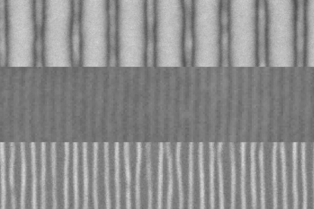
The result is four or more lines, each of them a fourth as wide, in place of the original pattern line. The combination of the lithographed layer and the top layer is what controls both the orientation and the alignment of the resulting finer lines, according to the researchers.
The top layer can also be additionally patterned, so the system can be used to build complex patterning, as needed for the interconnections of a microchip.
According to the MIT team, the new process can be implemented using existing machinery with only small changes. This could make the technology more appealing to chip manufacturers, compared to using new lithography techniques to print much finer patterns.
“Being able to create sub-10-nanometer features with polymers is major progress in the area of nanofabrication,” said Joerg Lahann, a professor of chemical engineering at the University of Michigan, who was not involved in this work. “The quality and robustness of this process will open an entirely new area of applications, from nanopatterning to nanotribology,” he added.
One roadblock that the DSA technique could face is the fact that the lines formed by the chemical reactions may form structures that are too regular. The DSA technique may not work very well for chips with more irregular patterns, such as CPUs, but may work well enough for chips with much more regular patterns, such as memory chips.
Lucian Armasu is a Contributing Writer for Tom's Hardware US. He covers software news and the issues surrounding privacy and security.
-
Litho59 While DSA is pretty amazing the dislocation defects encountered are at far to high a level for use in volume manufacturing.Reply -
mavikt @LITHO59Reply
Furtunately such nuisances didn't prevent Edison from promoting the light bulb. -
Litho59 An interesting comparison as in the early days Edison, I believe, promoted the light bulb a reviewer at a time, for a time just shorter than the time to failure of the filaments. Preservation did see that great invention succeed. Search SPIE papers on DSA for more info on challenges and probable limitations.Reply -
cats_Paw "As we approach the size of atoms".Reply
Am I the only one who is wondering how is it possible we went forward so much in that area, and so little in others?
I mean... Atoms guys... Atoms... -
hdmark @cats_paw yet comcast cant fix my internet :p (which seems to be close to the same speed i was getting 15 years ago)Reply -
JamesSneed Reply19490283 said:"As we approach the size of atoms".
Am I the only one who is wondering how is it possible we went forward so much in that area, and so little in others?
I mean... Atoms guys... Atoms...
People like computers pretty much universally even if it is just a "phone". So tons of money has went into chip design over the last 20 years. Now if we just had similar funding for other really big impact things like energy production. -
thelazy_1 How about fiber-optic transistors? The speed of light goes up to 765 terahertz as I recall.Reply
