Research Suggests Semiconductor Nanowires Can Unlock Ultrafast Transistors
Faster, more power efficient chips for our future machines

A collaborative team of researchers with the Helmholtz-Zentrum Dresden-Rossendorf (HZDR), the TU Dresden, and NaMLab has demonstrated significantly enhanced electron mobility in nanowires when these are put under tensile strain. An important metric for transistor performance, the increased electron mobility is expected to provide significant performance, thermal and power efficiency improvements that could unlock even faster transistors for future chips.
Crucially, the research works on well-known materials in the semiconductor space: the research focused on gallium arsenide nanowire structures, a compound that's already widely used in industrial manufacturing, and known to have a high intrinsic electron mobility. The research, published on Nature, takes advantage of a unique property of nanowire-based transistor designs, in that they can be subject to tremendous amounts of elastic strains without its atomic structure being damaged.
“We influence the effective mass of electrons in the core. The electrons become lighter, so to speak, which makes them more mobile,” explained Dr. Emmanouil Dimakis, scientist at the HZDR’s Institute of Ion Beam Physics and Materials Research. “We knew that the electrons in the core ought to be even more mobile in the tensile-strained crystal structure," he continued. "But what we did not know was the extent to which the wire shell would affect electron mobility in the core. The core is extremely thin, allowing electrons to interact with the shell and be scattered by it.”
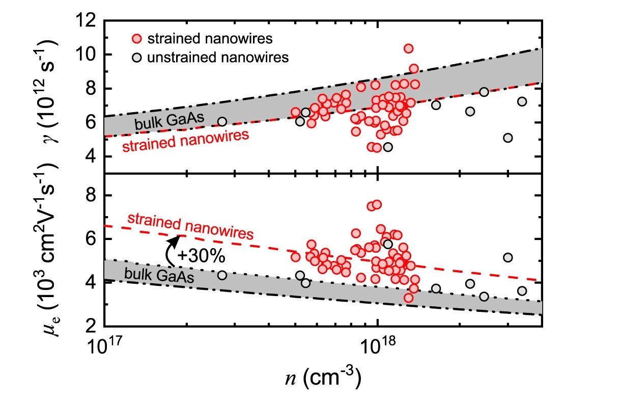
The team achieved this by enveloping the gallium arsenide nanowire cores in an indium aluminum arsenide shell. Due to its different atomic arrangement, the shell imposes elastic strain on the cores. The research proves that these higher levels of applied elastic strain on the core of gallium arsenide nanowires can improve electron mobility by at least 30% when compared to traditional strain-free or bulk gallium arsenide solutions (which Intel itself has already explored). The researchers theorize their nanowire design could even unlock a 50% improvement in electron mobility, furthering the advantages of their design. It looks like tension doesn't only accelerate changes in humans.

Materials and design research abounds in the semiconductor industry, with multiple teams of industry and research specialists racing towards more effective, performant, and scalable designs in this ultracompetitive space. As performance requirements push existing technologies to their limits, research is increasingly focusing in more exotic solutions. These have to be balanced for resource availability and cost (two of the reasons silicon is the current material of choice) as well as compatibility with existing manufacturing tools and techniques, in order to reduce the required, billion-dollar investments required for cutting-edge fabrication facilities.
The team is now looking to develop the first working prototype designs arising from their research. They're now planning to optimize the nanowire sizes and pitch, as well as the effects of doping (adding additional elements, such as silicon, to the compounds) in the search for that 50% electron mobility improvement they've already theorized.
Get Tom's Hardware's best news and in-depth reviews, straight to your inbox.

Francisco Pires is a freelance news writer for Tom's Hardware with a soft side for quantum computing.