Intel May Bet on Stacked Forksheet Transistor Tech for Sub-2nm Chips
Showcasing improvements at the level of a node jump.

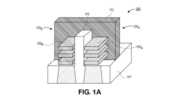
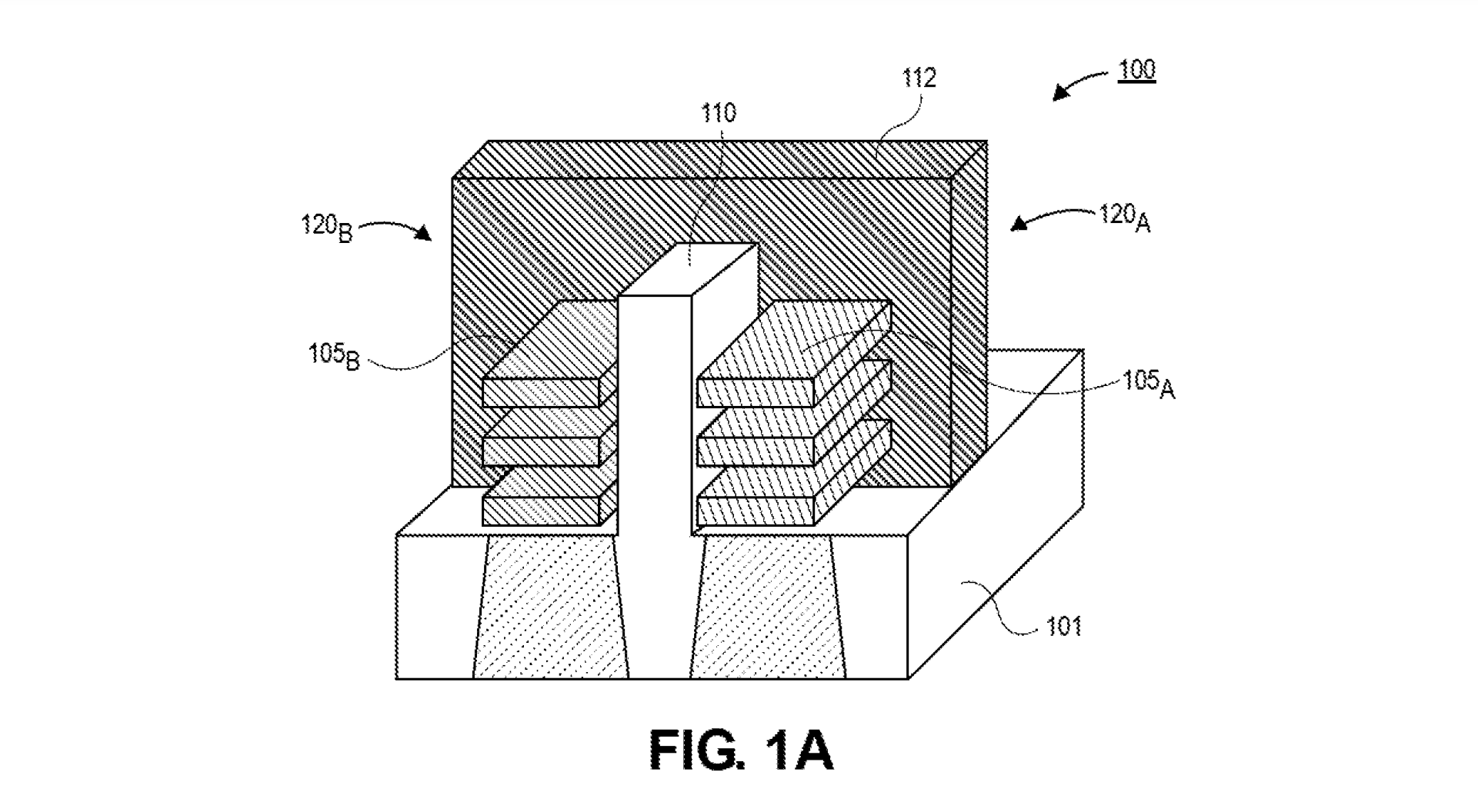
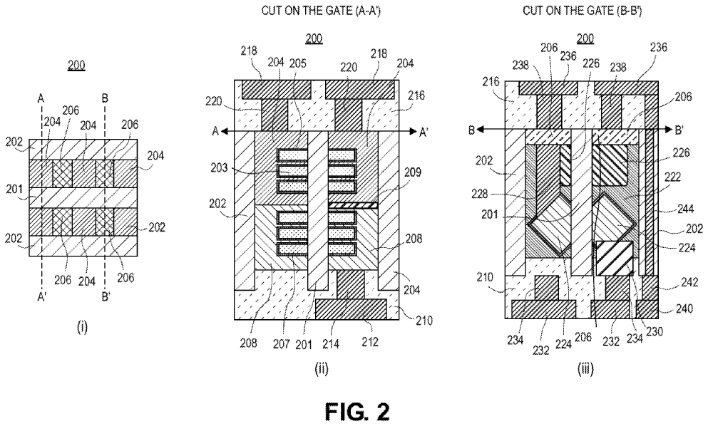
Intel may be setting its sights on a new transistor design as the Macedonian cavalry to its sub-2 nm manufacturing aspirations. A recently published online patent seems to point Intel’s way forward in keeping Moore’s Law alive via what it calls “stacked forksheet transistors.” However, the patent is fuzzy, as they tend to be, and Intel makes no claims on PPA (Power-Performance-Area) improvements.
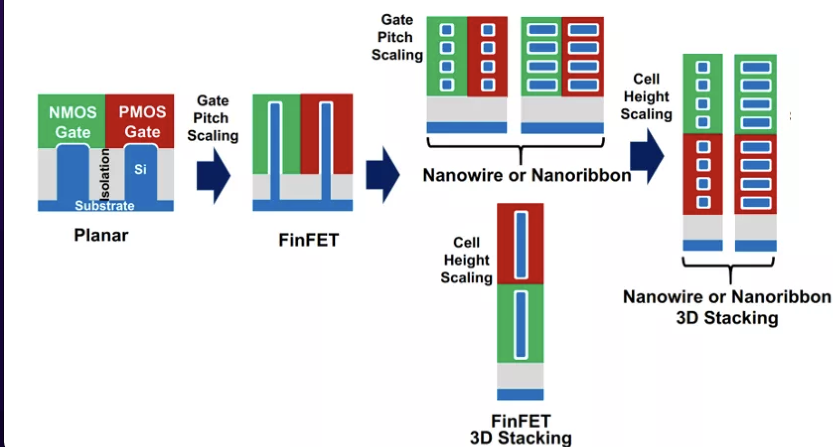
According to the blue giant, the new transistor design can ultimately lead to a 3D, vertically-stacked CMOS architecture that allows for increased transistor counts compared to today’s most advanced tri-gate designs. However, the difficulties of further shrinking transistors have become such that even Intel’s patent describes the constraints as “overwhelming” - the cost, risk, and complexity all now seem to outweigh potential benefits.

Intel's patent describes the usage of nanoribbon transistors paired with a new, atoms-thin germanium film that acts as a dielectric wall. The wall serves as a physical separation between the layers, acting as an insulator between the p-gate trench and the n-gate trench. It is repeated through each of the vertically stacked transistor layers, depending on how many transistors are being stacked upon one another. In practical terms, this allows for much tighter spaces between the P- and NMOS devices before their functions are affected (compared to how apart they'd have to be for the same effect without the wall), meaning Intel can fit more of them into a smaller area. As a result, Moore's Law just took another breath – albeit a ragged one as yet.
Intel had already begun exploring the technology as early as 2019 – the company presented on it at its Electronic Devices Meeting (IEDM) event. However, neither on this patent nor there can we find concrete data on some "hard estimates" on how forksheet tech can improve transistor density, performance, and power efficiency.
Luckily, Intel isn't the first company to reference this fabrication method. Imec, a Belgium-based research group, announced the development of the first standard cell simulation results for "forksheet devices" in 2019 as well – and yes, these forksheet devices are the basis of Intel's patent. So it's no surprise that two institutions have close and long-lived ties in nanoelectronics.


According to Imec’s first standard cell simulation results, when applied to a 2nm technology node, the technology can provide significant improvements in transistor density compared to traditional nanosheet approaches. We’re looking at a 10% speed increase or a 24% energy efficiency improvement at constant speeds, paired with a “more than 20 percent cell area reduction.” In addition, the Static Random Access Memory (SRAM) footprint (that usually makes up a CPU’s cache and is one of the most significant contributors to die area) receives an impressive 30% reduction.
Compare that with TSMC’s announced improvements of its 3nm node compared to 5nm: a 10 to 15% performance gain (at the same power and transistor count), up to 30% power reduction (at the same clocks and complexity), up to 70% logic density gain (suitable for cores), and an up to 20% SRAM density gain.
Get Tom's Hardware's best news and in-depth reviews, straight to your inbox.
We must remember that not all patents ever make it into actual products or fabrication technologies – they are sometimes ways to protect a potential or tentative investment or research venues or even metaphorically burn competitors’ advancements in that terrain. However, Imec’s research from 2019 already presented impressive possible improvements for a sub-2nm node, especially when considering that it’s within the exact etching resolution but with a different transistor architecture. So it’s jump – without a node jump.
Intel has now had the time to get much more research under its belt, and we now know research on stacked forksheet transistors continued until at least June 2020. And we also know that semiconductor manufacturing planning and research are incredibly long-tailed. Intel’s CEO, Pat Gelsinger, first mentioned 10 nm technology – now Intel 7 – in 2008, when he still served as CTO, citing he saw “a clear way” towards it. That clear way only truly manifested in this year’s Alder Lake, which goes to show the capital requirements of leading-edge semiconductor fabrication. Intel 7 may have come late, but has Alder Lake beating overclocking world records left and right.
It’s unclear whether Intel will opt for a stacked forksheet architecture in a 2nm process or if it would be looking to reap its design benefits earlier. But Intel filed the patent application, which ultimately means the design has some merit. Unfortunately, it seems the company knows more than we do about how viable the technology could be.

Francisco Pires is a freelance news writer for Tom's Hardware with a soft side for quantum computing.
-
helper800 I am not super in on the marketing of "2nm" transistors, but the traditional definition is that they have 2nm of space between between themselves, right? I thought there was some sort of unresolved barrier at 2-4nm density due to some quantum physics related issues? Again, I am not the most informed as far as this goes. Is this actually a 2nm process in the traditional sense or is it marketing attached to a Xnm process?Reply -
jkflipflop98 The nm metric is largely useless these days. It's morphed through history depending on who is showing off what. For many, many years Intel always measured from the outside edges of the contacts. Then it somehow became the smallest freestanding structure you can build. Then it turned into the thinnest line you can expose. Now it's just a name that has nothing to do with anything and is used as a marketing gimmick.Reply