Intel at IEDM: Stacking Nanoribbon Transistors and Other Bleeding Edge Research
Intel opens up about its recent research projects
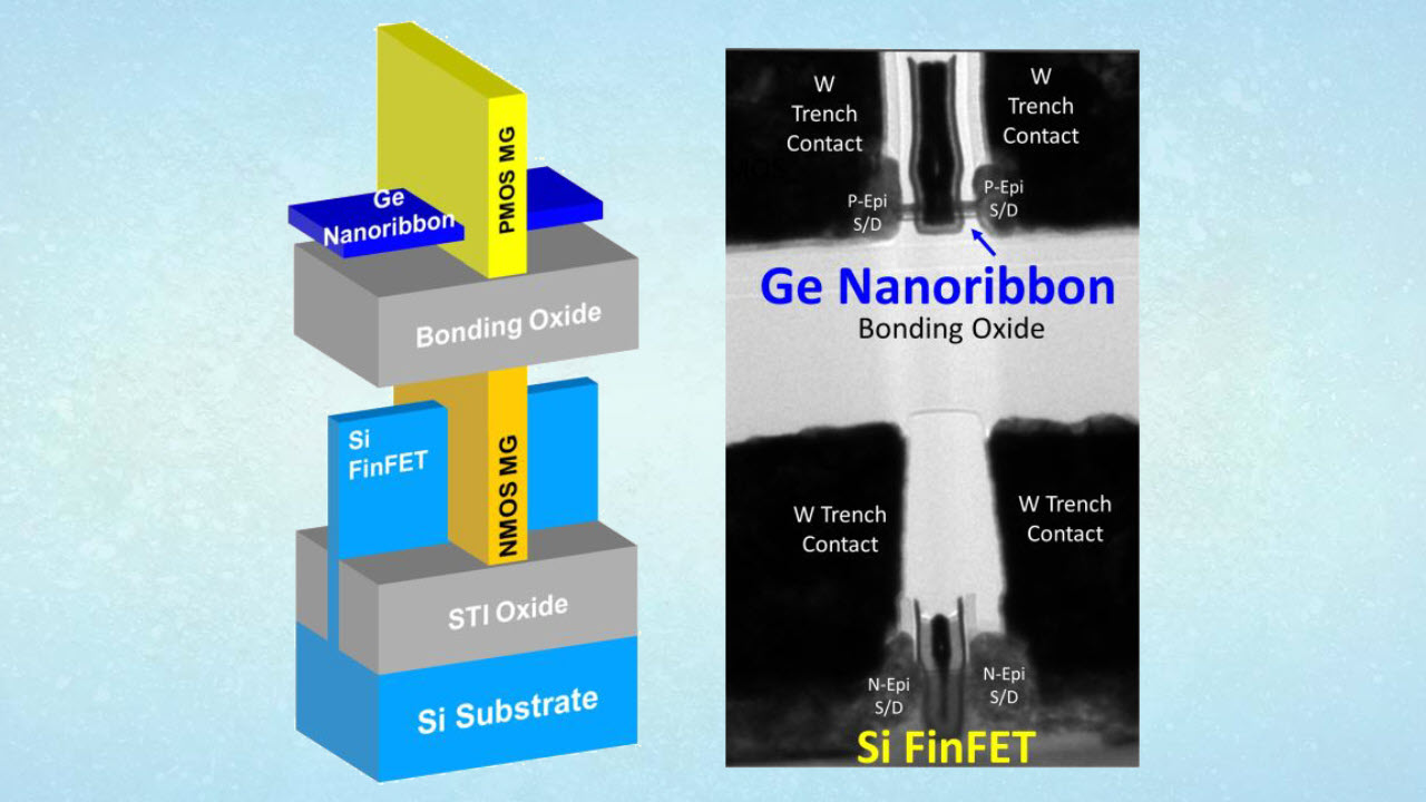
In a post on its Performance at Intel blog, Intel has outlined some of the research in 3D logic integration it has conducted and which it has presented at this week’s IEEE IEDM 2019 conference. The research includes the stacking of germanium nanoribbon transistors on top of silicon FinFETs and its Omni-Directional Interconnect that will succeed Foveros.
The blog was written by Robert Chau, an Intel Senior Fellow and director of components research. Seemingly having forgotten – or overcome – the company’s issues at 10nm, he argues that the future of Moore’s Law is brighter than ever “with more innovative technology options in the pipeline now than I have seen at any point in my career,” he wrote. (A sentiment that is shared by Jim Keller.)
He sees two areas that will drive Moore’s Law in the next decade, which he terms monolithic scaling and system scaling. The first is driven by classical transistor scaling and innovation, the latter by advances in packaging and interconnects.
At the annual International Electronic Devices Meeting (IEDM) this week, Intel presented papers on both topics. One thing those scaling vectors have in common is that they use the third dimension by stacking logic dies or even transistors on top of each other.
3D integration has been commonplace in the memory and storage space for some time now (with 3D NAND, HBM and 3D XPoint), and logic is now following in those footsteps. For example, Intel this year pushed the boundaries forward with Foveros to stack a 10nm logic die on top of a 22nm I/O base die.
While it is not necessarily sure that the presented research will reach commercialization (soon), it offers a glimpse of how the industry will drive Moore’s Law and integrated circuits forward in the years ahead.
Monolithic Scaling: 3D Transistor Integration
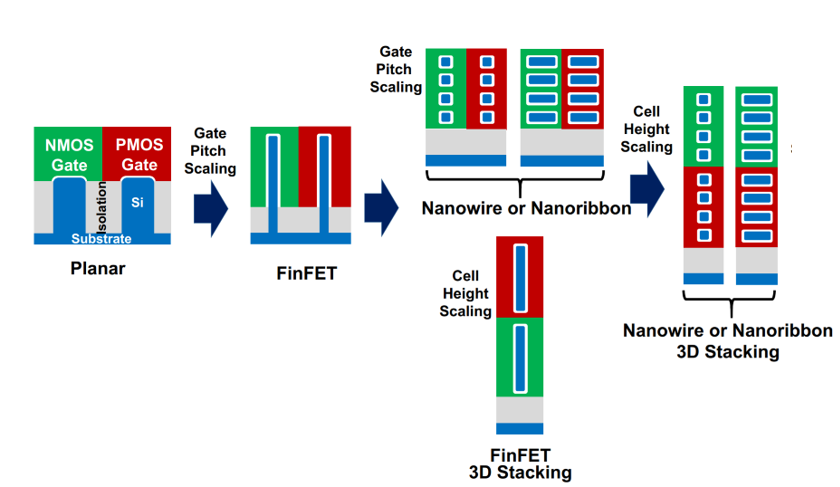
In CMOS technology, an NMOS and PMOS transistor are combined to create a device that – aside from leakage – only consumes energy when it switches its state. One problem that arises in process development, however, is that NMOS and PMOS don’t necessarily have all the same characteristics such as performance (drive current). In particular, the PMOS transistor typically lags in performance compared to the NMOS. In FinFETs, this can be solved brute-force by adding an extra fin in the PMOS transistor to generate extra drive current and improve its switching speed.
Get Tom's Hardware's best news and in-depth reviews, straight to your inbox.
Another possibility, which Intel’s research explored, would be to use a channel material with an intrinsic higher mobility: germanium. However, germanium is challenging to manufacture alongside silicon, which is why it hasn’t been used in favor of silicon.
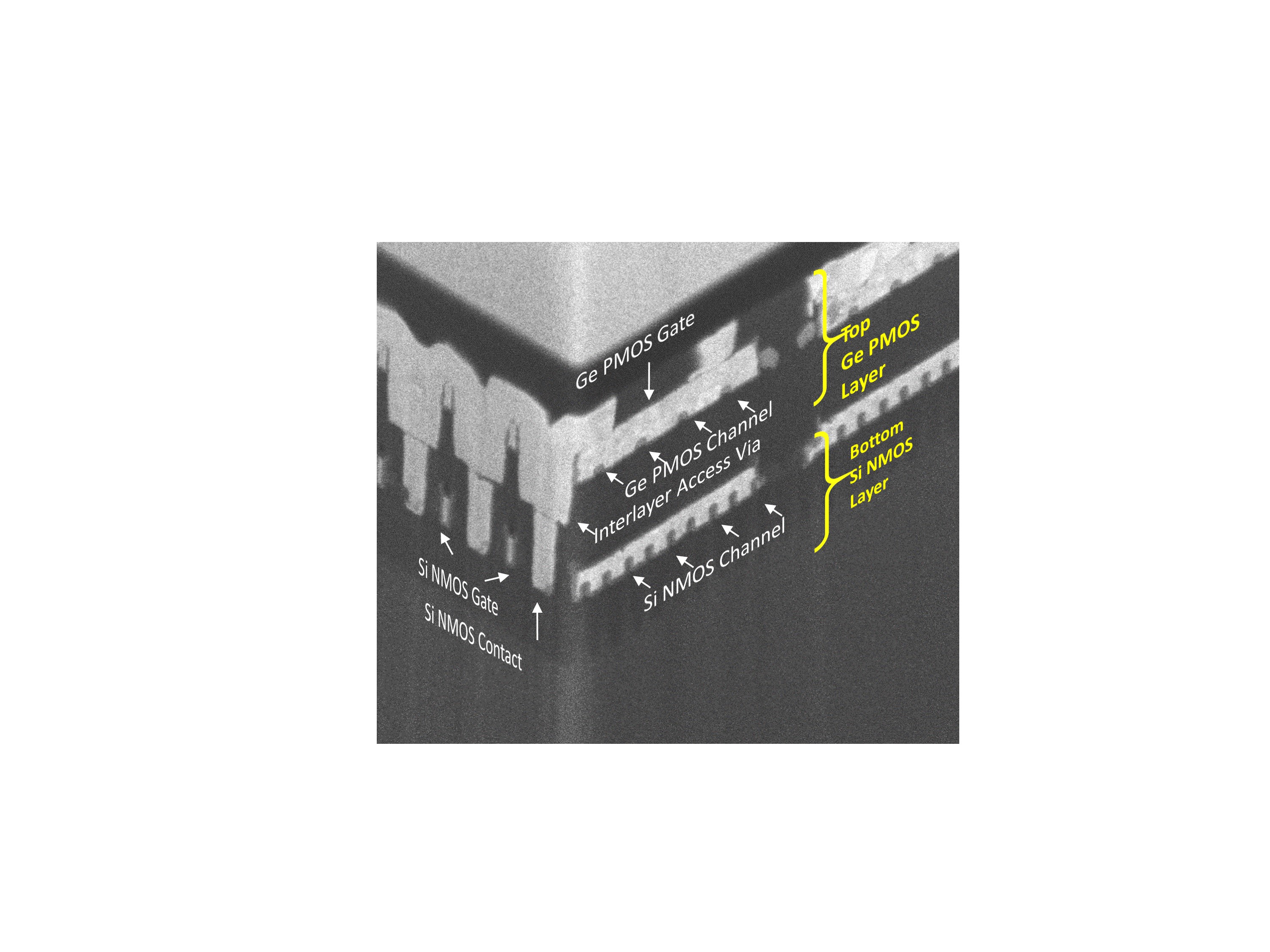
The solution Intel developed to circumvent this problem was a 3D sequential stacking architecture. The researchers first built a silicon-based NMOS device on the silicon wafer. Then, on a separate wafer, they fabricated a germanium film and bonded it on the first wafer, acting as a buffer layer. On this film, they built the germanium-based PMOS device.
This not only resulted in a PMOS transistor with “record setting” performance, it also provides essentially one step of Moore’s Law in transistor density since there are now two layers of transistors.
Nanoribbon Gate-All-Around Transistors
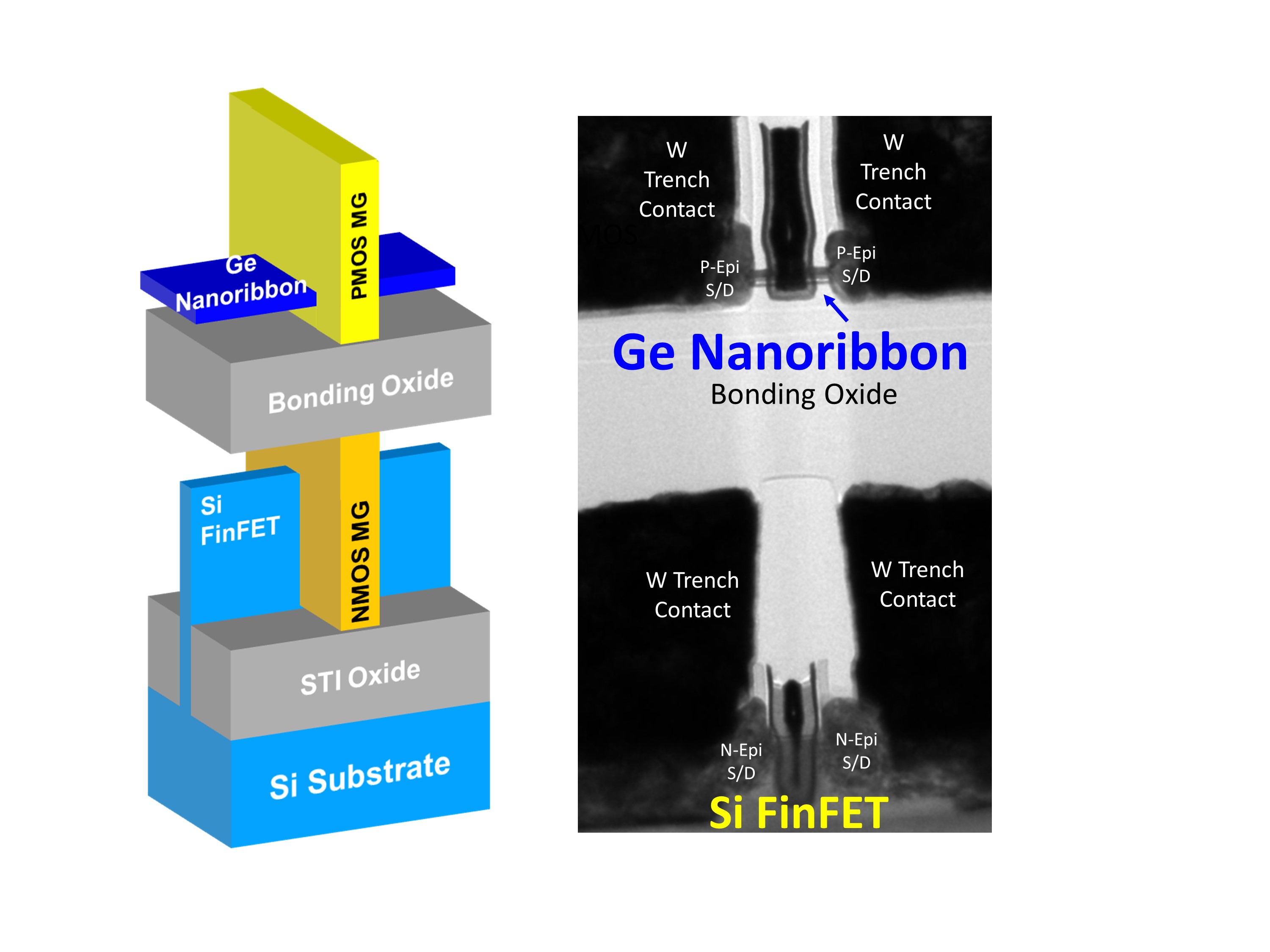
Moreover, the PMOS device was not a FinFET, but a germanium nanoribbon. A nanoribbon, also called nanosheet, belongs to the class of gate-all-around (GAA) FETs, where the gate fully wraps around the channel, as opposed to the FinFET where the gate goes around three of the four sides of the fin. As such, it is more of an evolutionary change as compared to the introduction of the FinFET that succeeded the planar transistor this decade.
Another common form of the GAAFET is the nanowire with a round channel. Gate-all-around transistors also can have both a horizontal (lateral) or a vertical orientation.
Intel is expected to introduce (some form of) GAAFETs at its 5nm process in 2023, perhaps followed by stacked PMOS and NMOS devices at 3nm in 2025 or 2026. If the company will opt for a mixed architecture, like in this research, remains to be seen.
In summary, compared to current commercialized chips, the researchers introduced the 3D stacking of heterogeneous PMOS and NMOS layers. The PMOS layer consisted of nanoribbons with a germanium channel, to remove the discrepancy in performance between the two devices. It had the highest reported performance yet for a germanium-channel PMOS transistor in an invertor test circuit. The NMOS layer remained a FinFET.
3D Heterogeneous Integration of GaN and Si
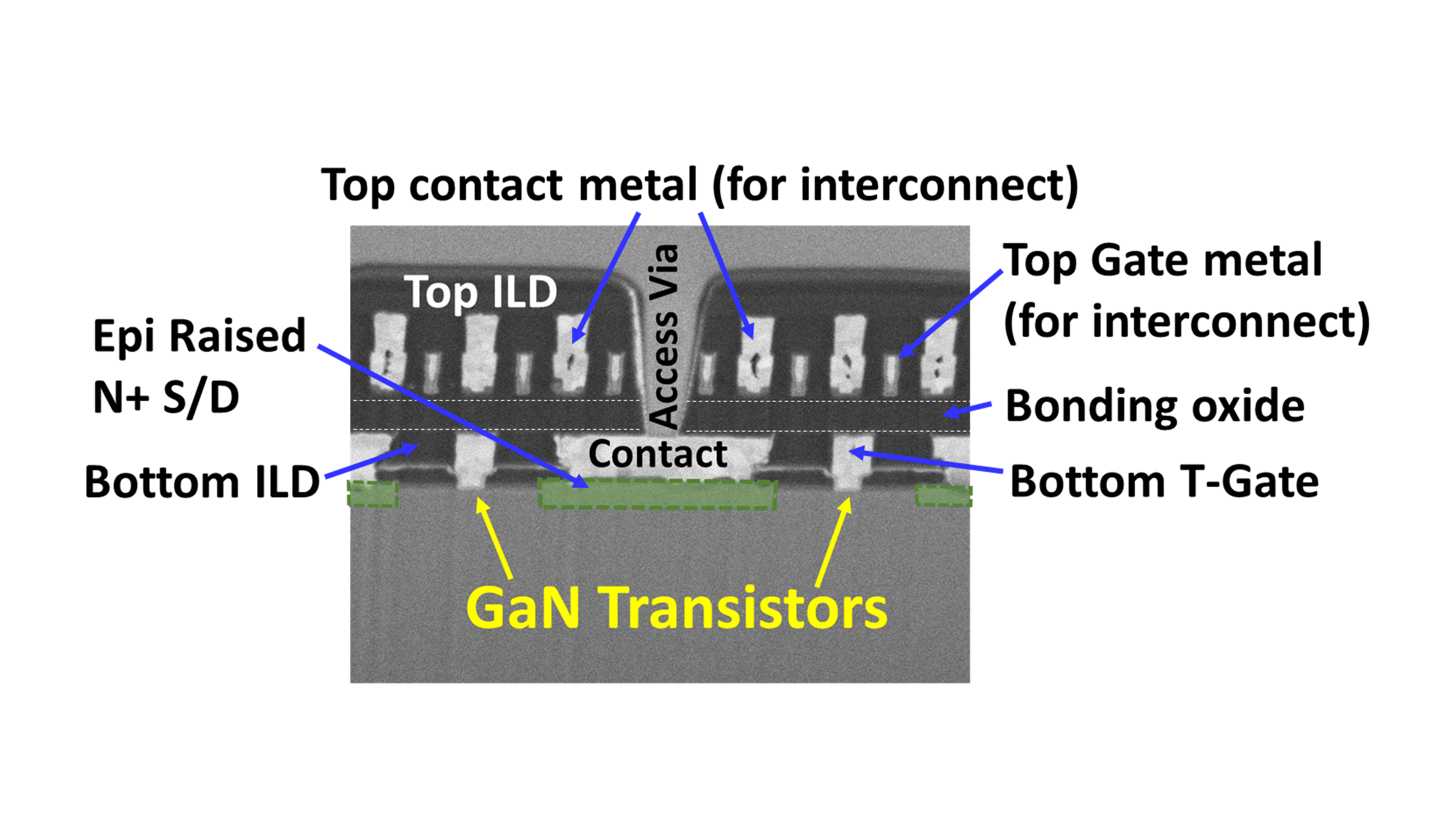
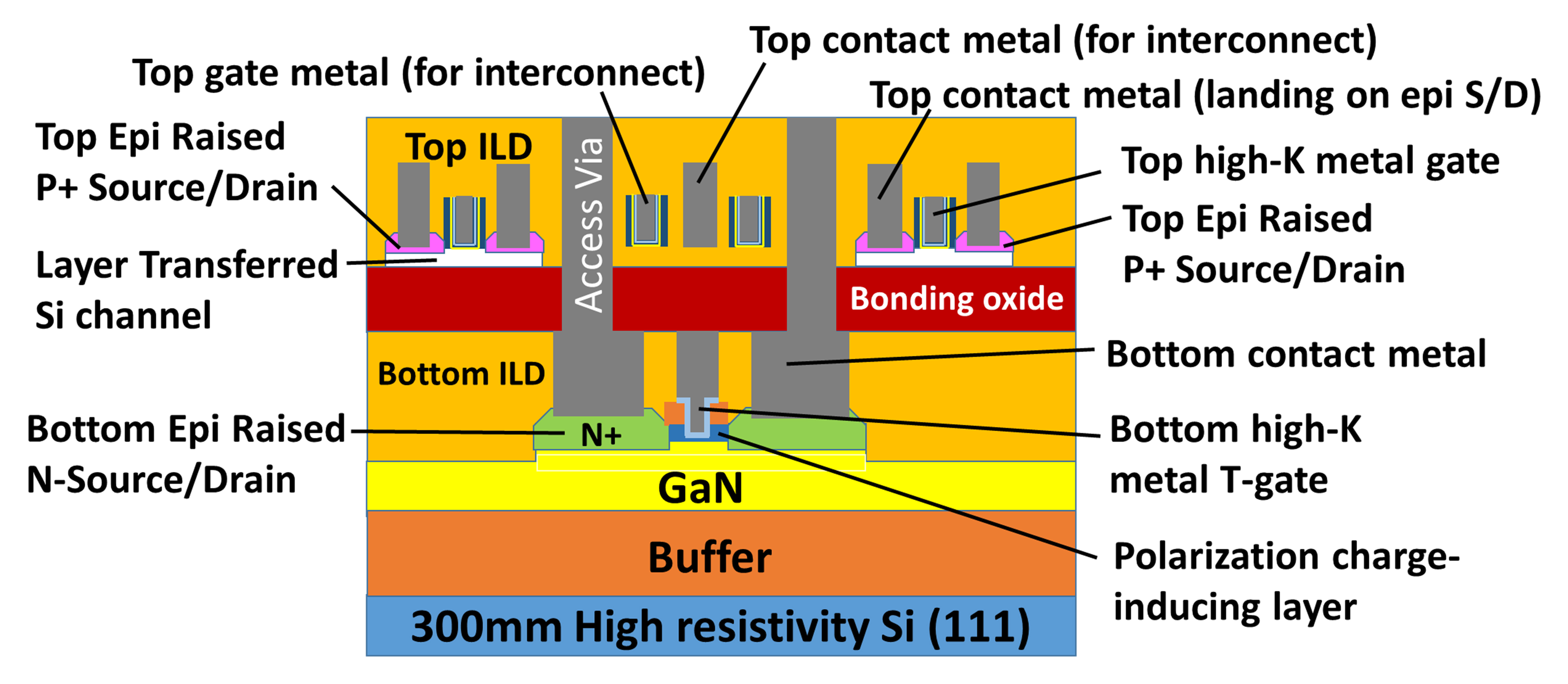
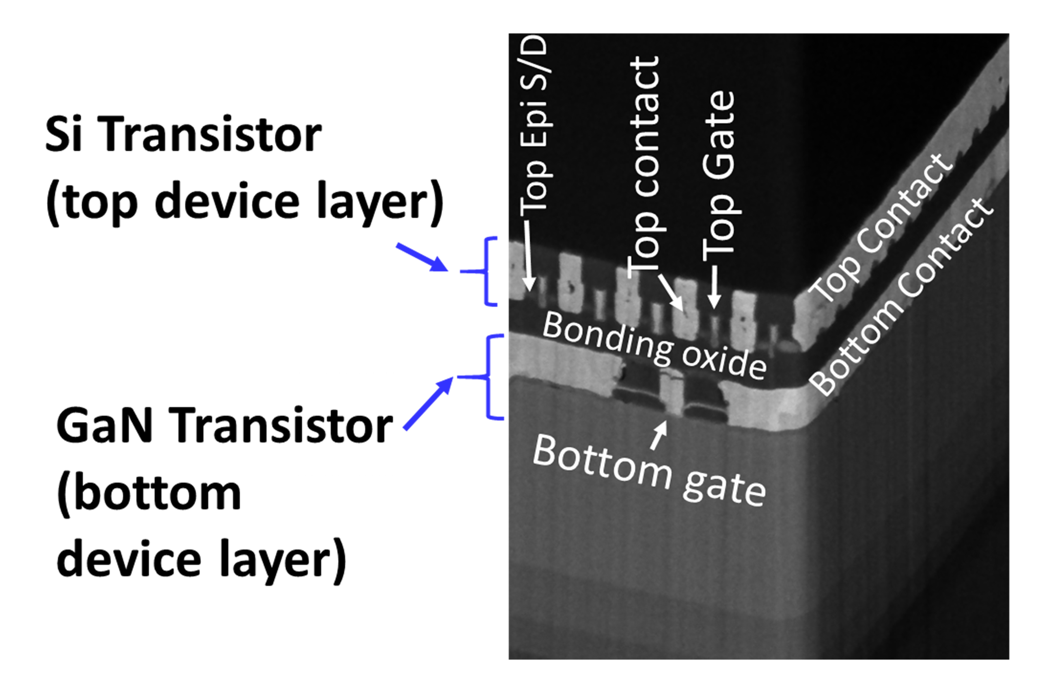
Intel also had a second paper on 3D heterogeneous integration as an example of monolithic scaling. In this research, an Intel team now stacked a standard silicon PMOS layer on top of GaN (gallium-nitride) NMOS transistors.
The goal here is to combine the best properties of both components on a single, compact chip. Silicon circuitry is optimal for digital signal processing, logic, memory and analog applications, while GaN has high-frequency, high-temperature and high-power attributes. In other words, it is most suited for RF and power delivery applications.
Such a 3D architecture would allow for the integration of (5G) RF front-end modules with standard SoCs, since those modules today are built as standalone units.

System Scaling: Omni-Directional Interconnect
In conjunction with its disclosures about its Foveros logic stacking technology, Intel this year also released information about how it will advance its packaging technology even further. With Co-EMIB, the company intends to connect multiple 3D Foveros stacks using EMIB to create systems “far larger” than the traditional reticle size limit. While Intel hasn’t officially disclosed it, the company has recently unveiled its Ponte Vecchio flagship 7nm discrete GP-GPU that uses Foveros and EMIB.
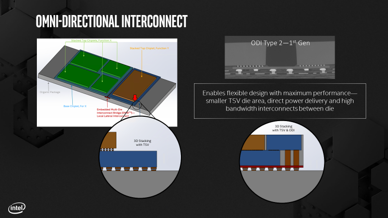
However, one hurdle with such large chips is power delivery, since Foveros uses tiny through-silicon vias. This is where Omni-Directional Interconnect (ODI) comes in. Intel says ODI offers the capabilities as Foveros for 3D face-to-face bonding, but uses much thicker wires for power delivery.
This allows chips to be packed much more tightly together. Intel gave three example configurations:
- A die partially buried, acting as a bridge between two other chips
- A completely buried die
- Two slightly overlapped dies
Closing Thoughts
When Intel delayed 10nm in 2018, it tried to reassure the public and stakeholders that it would have systems on shelves for the 2019 holiday season, while stressing the additional performance it had squeezed out of 14nm.
While those problems are by no means behind it, ever since its Architecture Day event a year ago, the company has been more optimistic, forward-looking and open about its plans ahead, including an annual cadence of new CPU architectures on both the PC and data center side; its ambitious plans for discrete graphics products and Mobileye; and on the process side, moving back to a two-year cadence of process technology introductions, with 7nm in 2021 using EUV and even a roadmap into 2029.
Intel’s problems have given AMD some breathing room on the CPU side to catch up and re-enter the data center, and for TSMC to capture process leadership (by Intel’s acknowledgment), but Intel’s message for the next decade is that innovation will resume relentlessly, at the beat of Moore’s Law, making it by no means clear or guaranteed who will lead in which segment in 2029.
Also at IEDM 2019:
- Intel demonstrates STT-MRAM for L4 cache applications
- Imec fabricates transistors with two-dimensional MoS2 channel
-
InvalidError Making pmos on germanium and nmos on silicon then bonding two wafers to make one chip from otherwise incompatible materials. We're getting into real fancy territory there.Reply -
digitalgriffin ReplyInvalidError said:Making pmos on germanium and nmos on silicon then bonding two wafers to make one chip from otherwise incompatible materials. We're getting into real fancy territory there.
I was thinking the same. It will be interesting to see how it deals with {atomic} P state differences which often generate heat. Stacking chips in such a manner is already problematic with cooling. Adding in different materials with different electrical shell potentials, will make things "very interesting" heat wise. -
TJ Hooker Reply
Can you elaborate on how a material with a different electron configuration would inherently generate heat, and how this would change by adding something like germanium? It would seem that "adding different materials with different electrical shell potentials" is something that is already done in conventional silicon CMOS, i.e. the dopants.digitalgriffin said:It will be interesting to see how it deals with {atomic} P state differences which often generate heat. Stacking chips in such a manner is already problematic with cooling. Adding in different materials with different electrical shell potentials, will make things "very interesting" heat wise. -
digitalgriffin Reply
Sorry for the long delay. Christmas vacation and all.TJ Hooker said:Can you elaborate on how a material with a different electron configuration would inherently generate heat, and how this would change by adding something like germanium? It would seem that "adding different materials with different electrical shell potentials" is something that is already done in conventional silicon CMOS, i.e. the dopants.
Whenever you send electricity from one material to the next electrons bump around atoms. The amount of ionization energy varies from one metal to the next. For example silver takes less energy than copper and is therefore a better conductor.
When you combine two different metals like a peltier junction and pass a current through them an interesting effect happens. One side gets hot. The other cold.
This is also the reason intel swithed away from using copper wire interconnects to the package. Colbalt was closer to the native silicon in characteristics. Not only this but it reduced signal reflection due to micro differences in resistence.
That said doping of cmos transistors is a very effective way to create low power but slower circuits. Doing so over a long distance though creates the same issues. Because you are going from mat a to mat b to mat a, i would imagine the heating and cooling would cancel each other out. There are inefficiencies though and it generates heat. But i dont know the physics of why its more efficient for intel. Hence the mystery for me.
I always imagined a transistor like this...youre running along a road and you come up to a river. You cant cross that river till you have something to hop off of, like a floating raft in the middle. (Base) The bigger the float raft the more can go at once by bounce skipping off it. But if the river gets too wide (distance between collector and emmiter) you slow down and need more push (voltage). So while the raft allows you to cross the divide, it isn't as efficient as a solid road.
Im going to be honest and tell you this isnt my specialty. I do design some circuits but some basic sensors and data acquisition circuits.
