Nvidia Exploring Various Multi-Chip GPU Designs
Divide and conquer

Nvidia researchers have published an article detailing the various ways the company is exploring how Multi Chip Module (MCM) designs can be deployed for future products. As computing becomes more and more heterogeneous, Nvidia seems to be looking for a way to add flexibility to its semiconductor designs. This could be achieved by "mix and matching" different hardware blocks according to the intended workloads, and that's exactly where MCM comes in.
The first factual information on AMD's research into MCM came to light in 2017, when the company demonstrated how an MCM design with four chiplets could outperform the biggest monolithic GPU that could be built at the time by a whopping 45.5%. Cutting up a large die into several smaller ones helps improve yields (smaller dies have fewer chances of having critical manufacturing defects), and also allows for more computing resources to be chained together than a single, monolithic die ever could. Of course, being smaller, these chips should also present better thermals and power efficiency than their larger brethren.
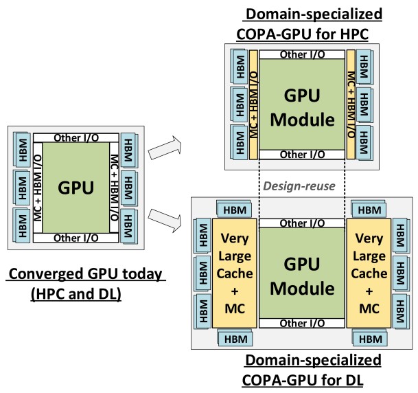
Nvidia's doubling-down on MCM GPUs is called the Composable On Package GPU, or COPA. This latest research piece is more concerned with how Nvidia will handle the increasing differentiation between HPC and AI workloads, which have been drifting apart for a while now. Clearly, Nvidia is concerned that its single-product approach (read: the GA100 accelerator and its predecessors) will start losing ground towards the increasing workload specialization in those areas.

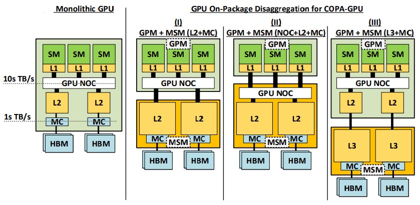
To that effect, Nvidia has been simulating how different MCM designs and configurations could allow it to mix and match the required hardware blocks for each workload. The paper shows how a 25% memory bandwidth reduction actually only slows down HPC workloads by an average of 4%. Cutting the available bandwidth by a further 25% added another 10% performance penalty. So with 50% less memory bandwidth (and removing the hardware that enables it), Nvidia can claw back chip space for other, more appropriate hardware blocks that would deliver more performance than has been lost for the appropriate workload.
Not all hardware blocks are made equal, however. Certain hardware blocks can't currently be separated without incurring extreme performance penalties. COPA is Nvidia's attempt to simulate the effects of multiple chiplet design decisions, and how they relate to performance.
The company's approach prioritizes the high-margin HPC and AI markets first, which makes sense, especially considering how multiple companies have been encroaching on that space with their own custom solutions (for example, Cerebras with its Wafer Scale Engine and Lightelligence with its photonics-based PACE). However, this same workload-semiconductor philosophy can be applied across Nvidia's GPU-based product stack, including consumer GeForce.
MCM for GeForce does present more difficulties, of course. Scaling workloads that are already designed to be split up across potentially thousands of nodes in a supercomputer is inherently different from scaling real-time gaming workloads. In fact, Nvidia has basically pulled the plug on SLI (scalable link interface) multi-GPU gaming solutions. MCM will need higher interlinks between the various GPU blocks if it's to be usable for gaming without the need for duplicated resources and alternate frame rendering.
AMD has already shown us what MCM can do for cost, power, and performance in the CPU space with its Zen architecture and subsequent iterations. MCM in GPUs is arguably a more difficult achievement, but technology will get us there. When it does, Nvidia will be composing GPUs out of multiple IP hardware blocks, employing a modular approach to chip design, and will likely have a much more specialized product portfolio according to the computing needs of the time.
Get Tom's Hardware's best news and in-depth reviews, straight to your inbox.

Francisco Pires is a freelance news writer for Tom's Hardware with a soft side for quantum computing.
-
VforV Yeah, they need to "explore" harder because AMD already shipped their server MCM GPUs and soon™, later this year Radeon will have RDNA3 gaming GPUs with MCM and still nvidia will be on monolithic design. Good times.Reply -
spongiemaster Welcome to 2019.Reply
https://www.pcgamesn.com/nvidia/graphics-card-chiplet-designs
“This gives us a bunch of technologies on the shelf that at some point in time,” says Dally, “if it became economically the right thing to do to, assemble GPUs from multiple chiplets, we basically have de-risked the technology. Now it’s a tool in the toolbox for a GPU designer.” " -
Endymio Reply"Of course, being smaller, these chips should also present better thermals and power efficiency than their larger brethren... "
Article quality has degraded markedly as of late. Die size does not affect power efficiency. Nor does it improve thermals, if those smaller chiplets are combined into an equivalent-sized package. NVidia's COPA is about flexibility and yields, nothing more. -
renz496 there are interesting read at next plaform. it seems going forward nvidia might end up making two type of compute card. one for HPC and one for AI. then nvidia will optimize the design based on it's need (HPC or AI) . although the next platform said the industry want one chip solution that is exceptional at both HPC and AI task.Reply