Is Nvidia Not Being Forthcoming About Lower-Speed MX150 GPUs?
Get Tom's Hardware's best news and in-depth reviews, straight to your inbox.
You are now subscribed
Your newsletter sign-up was successful
Nvidia appears to be feeding OEMs two different versions of its MX150 mobile GPU, and it has been less than forthcoming about the performance differences.
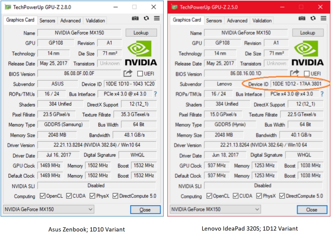
As first reported by Notebookcheck, there are apparently two different variants of the GeForce MX150 in the wild. These differences are easily identifiable in a pair of GPU-Z screenshots taken from an Asus Zenbook laptop and a Lenovo IdeaPad 320S Ultrabook. The Zenbook sports a MX150 GPU with the device ID of 10DE 1D10, whereas the IdeaPad is labeled as 10DE 1D12. The publication also claimed to have only found the 1D12 variant in 13” Ultrabooks so far, including the HP Envy 13, Asus Zenbook 13, and Xiaomi Mi Notebook.
Although the memory capacity and CUDA core count of the MX150 GPUs are identical, the clockrates (and therefore, performance) are vastly different, with the 1D12 GPU downclocked (in comparison to the 1D10) by 523MHz, 494MHz, and 249MHz on the base, boost, and memory clocks, respectively. The report also asserted the MX150 variants have different TDPs, with the 1D10 sitting at a 25W TDP and the 1D12 drawing less than half that at 10W.
Article continues belowThe difference in clock rate and power consumption of the 1D12 version are similar to the differences found in Nvidia’s Max-Q graphics, which allows powerful GTX-branded GPUs (such as the GTX 1070 and 1080) to fit into smaller devices by lowering the power ceiling and GPU clocks via firmware. However, Nvidia plainly advertises these differences with the higher-end GPUs, and the company doesn’t appear to have any differentiated marketing materials for the two MX150 GPUs.
To be fair, Nvidia’s GeForce MX150 specification page clearly notes that GPU implementation will vary by OEM, and that consumers should refer to respective vendors’ websites for actual shipping specifications. We're accustomed to seeing differences in memory capacity in these situations, and the statement suggests that OEMs are ultimately in control of how to utilize the GP108 GPU that Nvidia ships them for use in their products. This could mean that Nvidia isn't to blame for the lack of transparency, but the differentiated clock rate and device ID indicate that this is implemented at a firmware level, which more or less shifts responsibility back to Nvidia (which provides the firmware).
We’ve reached out to Nvidia for comment and will update this article if and when any new information is available.
Get Tom's Hardware's best news and in-depth reviews, straight to your inbox.
Derek Forrest was a contributing freelance writer for Tom's Hardware. He covered hardware news and reviews, focusing on gaming desktops and laptops.
-
King_V I guess it would be too much to expect that maybe the differentiation should be treated the way they do with the 1070 and 1080 variants?Reply
Or, maybe, you know, something like the powerhouse being the MX150 and the lower level ones MX150E or MX150U or somesuch? -
MCMunroe I would be fine if this was done at a software level. Then users who cared could change it knowing it would effect battery life, temps, and noise. This how ever is very shady.Reply
I am a bit PO'd that my XPS 15 has a GTX 1050, with voltages and power locked, as well as missing half the ROPs: 16 (vs 32). Device Id: 1C8D. -
Olle P In what way does this differ from the CPUs that are run at different TDPs depending on settings in the UEFI?Reply
Here it's a firmware setting, which just about anybody can change(?) using some OC software... -
MCMunroe @OLLE P- The GPU and the CPUs you speak of have firm TDP limits. It will current throttle even if you set the clocks faster. (why can't I delete my double post? Sorry my bad)Reply -
cryoburner Reply
If the laptop's cooling system is only designed to handle a 10 watt GPU, then you might not be able to get much higher than that anyway. Clearly, this low-power version should be given a given name, so that consumers can make informed decisions when comparing laptops.20817575 said:I would be fine if this was done at a software level. Then users who cared could change it knowing it would effect battery life, temps, and noise. This how ever is very shady. -
oldschoolbluesplayer * * * Also look at the difference in the *Pixel Fillrate and the *Texture Fillrate...Reply -
10tacle Well are the technical specs of each mGPU stated by the laptop OEMs in their product description technical specs list? Places like on the box packaging, in the manual, and on their websites? If not, then perhaps Nvidia needs to get with the OEMs and advise them to detail those specs on their various models so consumers do not think they are getting one or the other chip as everyone has their own needs - some want lower power with less performance but longer battery life, others want more power being plugged into the wall for example.Reply
Perhaps Nvidia can simply just clear up any reference confusion as someone said above and just needs a letter on end of each GPU identifying each. Then Nvidia can reference the info of each mGPU in specs on their website with the hard stamped fabrication performance numbers that are set in BIOS OEMs cannot control with these:
ROPs/TMUs
Shaders
Texture Fillrate
Pixel Fillrate
Bus width
Memory size
Memory bandwidth
^^Those don't change by the laptop OEMs here as the article mentions and Nvidia should put that hard data on their website for each mGPU. Nvidia even lists most of these factory specs for their dedicated GPUs under each model. Just the GPU clock, memory speed, and memory boost speed are set by the OEMs here by the AIB OEM partners so those specs are up to them to report.
This is an easy fix by both parties and doesn't need to cause confusion. I don't think they were doing anything illicit. It just appears to be another oversight disconnect between engineering and marketing (yet again). -
MCMunroe Reply20819251 said:Well are the technical specs of each mGPU stated by the laptop OEMs in their product description technical specs list? ...
ROPs/TMUs
^^Those don't change by the laptop OEMs here as the article mentions and Nvidia should put that hard data on their website for each mGPU.
I just checked on Nvidia's website. The listed mobile specs for the GTX 1050 laptop do not mention half the ROPs of the desktop model. I assume that's why it is benchmarking far lower than GTX desktop 1050's and laptop GTX 1050 Ti's than the difference in shaders and clocks suggest.

