Deep Dive: Nvidia Inference Research Chip Scales to 32 Chiplets
Get Tom's Hardware's best news and in-depth reviews, straight to your inbox.
You are now subscribed
Your newsletter sign-up was successful
Nvidia has presented a scalable multi-chip module (MCM) inference research chip. The 4.01TOPS deep neural network (DNN) accelerator scales to 32 chips and 128TOPS, and is therefore suitable for applications ranging from mobile devices to the data center. The chip is fabricated on 16nm and was presented at the 2019 VLSI Symposium (PDF).
Nvidia took the stage this year at VLSI Symposium to present RC 18 (PDF) – Research Chip 2018, as WikiChip wrote. The chip is targeted at deep learning inference workloads. Inference, the task of applying a deep neural network to new data (like performing image recognition), is quickly gaining in importance, both at the edge in mobile phones and dedicated hardware, as well as in the data center with accelerators from both Qualcomm and Intel coming in 2020. The versatility of inference deployment is best illustrated by Intel’s inference portfolio, which consists of its Cascade Lake-SP Xeons with DLBoost, its FPGAs, integrated graphics, Movidius Neural Network Stick, Mobileye EyeQ chips for ADAS, and soon its dedicated NNP-I in M.2 form factor.
Overview
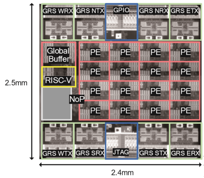
To cover a multitude of power, performance, application and form factor variables, Nvidia designed its inference research chip as a scalable MCM. A single chiplet has an area of just 6mm2 and contains 87 million transistors. The 36-chiplet MCM hence contains 216mm2 of silicon.
Article continues belowEach die contains 16 processing elements (PEs) connected via a network-on-chip (NoC), accounting for roughly half the area of the die. The rest of the die is composed of a network-on-package (NoP) router, a 64kB global buffer that acts as second-level storage, and a RISC-V control processor.
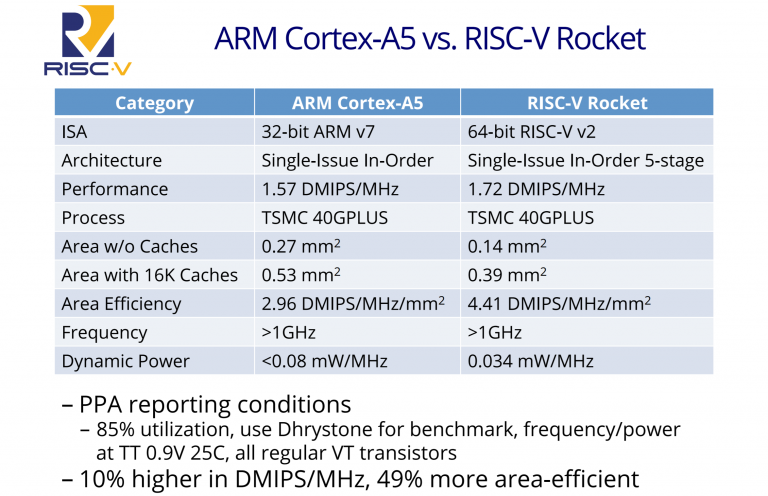
According to the paper, the RISC-V control core configures communication between PEs and global buffers via software-managed registers. It is a Rocket core, which is in performance comparable to the ARM Cortex-A5.
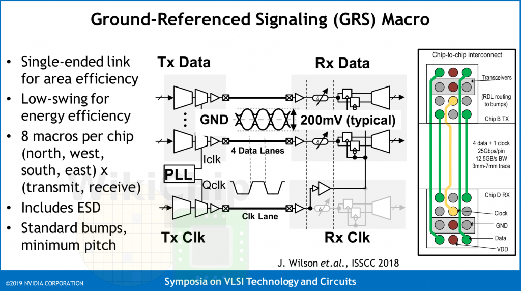
The dies in the MCM are connected in a mesh network. While the NoC routes between individual PEs, the NoP router transfers packets between the NoC and neighboring chips. This is done via four pairs of GRS transceivers: There are four receivers and four transmitters, one for each neighbor, each with a speed of 100Gbps.
Diving further into the GRS transceivers, GRS stands for Ground-Referenced Signaling, using the ground as reference voltage. This improves robustness and ensures that no noise is induced in the power supply. The link is single-ended, similar to DisplayPort. NVIDIA says it worked for over half a decade on this link, and envisions in the future it could use it to connect GPUs in a 2x2 array on a package with DRAM, then repeating the process with the packages. Such a board with 16 GPUs could then be further connected to other boards in a torus topology.
Get Tom's Hardware's best news and in-depth reviews, straight to your inbox.
This is similar to aFoveros-EMIB concept product Intel showed at its Investor Meeting in May, and also similar to how Intel intends to connect multiple of its upcoming Nervana Spring Crest chips, which are purposed for deep learning training.
For connecting the dies, Nvidia used a standard organic substrate for the MCM, since an interposer would be too expensive. The top-six dies are used for I/O to the outside world.
PEs and Performance
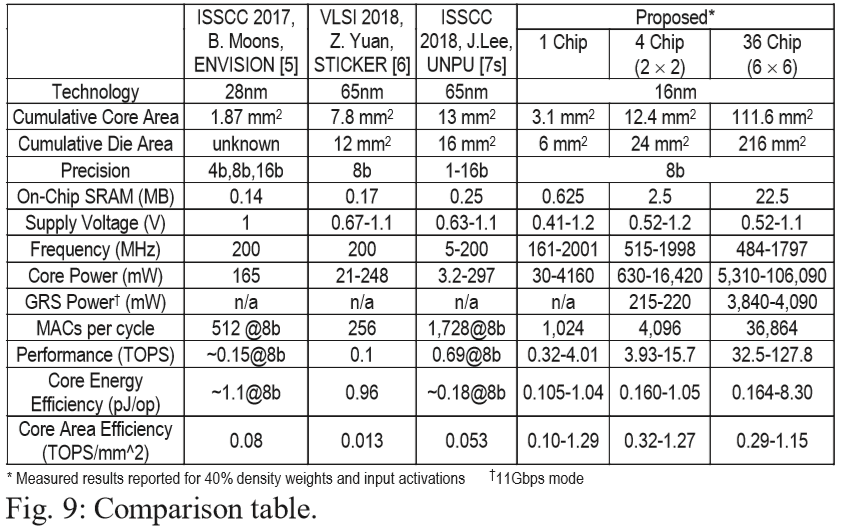
Each processing element contains eight parallel lanes of 8-way multiply-accumulate (MAC) units, each with a precision of 8-bit (as is getting common in inference). Since there are 16 PEs, one chip can perform 1024 MACs per cycle. At its maximum clock speed of 2.0GHz at 1.2, this gives a performance of 4.1TOPS (one MAC is two operations) while consuming 4.2W. The supply voltage can go as low as 0.41V.
In a 6x6 36-die configuration, the frequency is lowered to 1.8GHz, resulting in 128TOPS at 106W power consumption. To first approximation, this should be comparable in power and performance to the Xilinx Versal and Intel Agilex FPGAs, although those are built on a 7nm-class process node. The 36-chip system achieved a ResNet-50 score of 2615 images/sec at 0.85V. This is roughly comparable to four Google TPUv2s or four Tesla V100s. On AlexNet, 75% hardware utilization was achieved. The chip operates on one layer at a time.
Wrapping up
WikiChip Fuse notes that the chip does not have a memory controller. Instead, an FPGA is employed. WikiChip also argues that the chip could be made more balanced between interconnect and processing area by using a larger mesh with more processing elements.
The VLSI (Very Large-Scale Integration) Symposia on Technology and Circuits, as it is called in full, is one the leading annual conferences on semiconductor technology and circuits. Among the notable ones this year, TSMC and Intel each presented several papers.
TSMC talked about a 2D material PFET and presented two papers related to packaging, about its new SoIC (System on Integrated Chips) technology that is its equivalent of Intel’s Foveros, and another one about a dual-chiplet 4GHz octa-core research chip using its CoWoS interposer-based packaging.
Intel presented embedded RRAM on its 22FFL process (22FFL is an updated version of its 22nm technology with higher density, higher performance, lower power and ultra-low leakage transistors); a lightweight 14nm AES accelerator that is hardened against side-channel attacks; and a 10nm 112Gb/s PAM4 receiver with longer reach and smaller area than its previous work.
-
bit_user ReplyIn a 6x6 36-die configuration, the frequency is lowered to 1.8GHz, resulting in 128TOPS at 106W power consumption.
Hmmm... a RTX 2080 Ti is quoted at ~228 int8 TOPS in 260 W.
Source: https://devblogs.nvidia.com/nvidia-turing-architecture-in-depth/
So, not an absolute improvement. Efficiency-wise, that's 1.2 TOPS/W vs. 0.88 TOPS/W or a 38% improvement! However, the RTX card is 12 nm and this is 16 nm. And, if you compare the silicon area of 216 mm^2 (@ 16 nm process) the TU102's 754 mm^2 (@ 12 nm process), it's clear they're onto something.
BTW, nice article, Arne. IMO, it has just the right amount of detail and explanation.


