Intel Puts 10nm Ice Lake CPUs on an M.2 Stick, Meet the Nervana NNP-I Accelerator
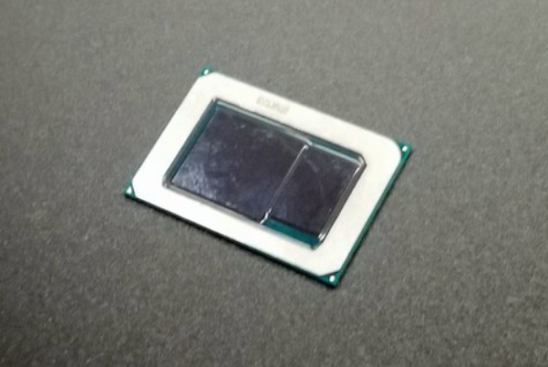
Intel announced here at its Israeli Development Center (IDC) Day in Haifa, Israel that its Nervana Neural Network Processor for Inference, of NNP-I for short, comes as a modified 10nm Ice Lake processor that will ride on a PCB that slots into an M.2 port (yes, an M.2 port that is normally used for storage). Intel also removed key portions of the Ice Lake processor, like the graphics cores and display blocks, to make room for AI accelerators.
The world of AI is upon us, poised to fundamentally change local compute on our phones, laptops, and desktops, but the majority of AI workloads still happen in the data center. Compute-heavy training workloads create complex neural networks that run object recognition, speech translation, and voice synthesis workloads, to name a few, but that's not where the work stops. The real key to employing the power of AI at scale lays in deploying the finished models to chew through the daily task of sorting and analyzing the world's data in a task called inference.
Inference workloads are much lighter than training, so they don't require the racks of powerful GPUs and FPGAs used to create the models, but like all forms of compute, it does eventually boil down to cost. That means performance-per-watt and cheap upfront pricing is more important for inference, and that's where Intel envisages its NNP-I accelerators slotting in (quite literally) to offload Xeon servers from inference-intensive workloads, thus freeing the bigger chip up for general compute tasks.
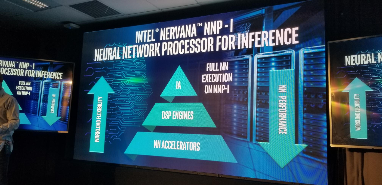
Intel took the base Ice Lake design (pictured above) and modified the processor's die to customize it for AI workloads. The device still uses the standard Ice Lake package with the CPU and platform controller hub (PCH) on a single board, but Intel removed the GPU and display blocks on the die and replaced them with a custom-designed AI engine tailored for specific types of inference code. The company also added DSP engines that it could use for algorithms that aren’t specifically tuned for the fixed-function accelerator blocks, affording a bit of needed forward-compatibility for the fast-moving AI space.
Intel hasn’t shared finer-grained details of the accelerator blocks, but they likely use a series of repeating elements, much like a GPU. With Gen11’s beefy memory subsystem (deep dive here) already in place to feed the beast, the company likely swapped out the graphics execution units (EU) with customized logic (or modified the existing units) while retaining the interconnects and complementary structures between the units.
The CPU still features several x86 Intel architecture (IA) compute cores, though Intel hasn’t provided a specific core count, that wield the Sunny Cove microarchitecture. Intel’s Oren Gershon, the GM of Inference Products Engineering, did vaguely mention that the company removed a few of the ‘other cores’ to make room for the extra componentry, so it is possible that these quad-core Ice Lake processors now function as dual-core models.
Get Tom's Hardware's best news and in-depth reviews, straight to your inbox.
Intel mounts the package on different forms of add-in cards, like the M.2 version pictured above, which can then slip into the standard M.2 port on a server motherboard, or on larger add-in cards that slot into a standard PCIe slot. Unlike some custom silicon designed for AI, like Google’s TPU, this device is broadly hardware-compatible with almost all existing modern servers. The approach is also scalable: You can add as many NNP-I’s to the server as needed, especially with PCIe risers that house multiple M.2 ports.
Intel says the NNP-I falls into a similar thermal design power (TDP) range as the Ice Lake processors, meaning they’ll top out around 28W, but noted that the M.2 interface’s 15W limitation hinders power delivery to the smallest devices. NNP-I’s connected to larger add-in cards can operate at the highest TDP ratings, meaning they offer much more performance.
Intel will provide software that orchestrates moving inference ‘jobs’ to the accelerator entirely, which will then notify the Xeon CPU when the work is done. The offloading eliminates the Xeon’s back-and-forth communication across the PCIe bus with other types of accelerators, which is taxing for the CPU because it generates interrupts and requires data movement. In contrast, the NNP-I works as a self-contained system with its own I/O accommodations (PCH) that allow it to access the data required for processing. AI workloads tend to ingest data voraciously, which would make the relatively slim PCIe 3.0 x4 connection seem like a bandwidth bottleneck, but Intel assured us that it has tested data-intensive video analytics workloads and didn’t encounter limitations. Instead, Intel said those classes of workloads are actually compute bound.
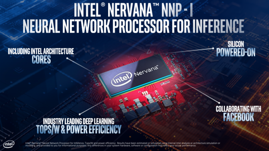
The x86 cores also support Intel’s VNNI deep learning instructions (aka DL Boost) that leverage AVX-512 to boost performance. Intel says that affords a final level of flexibility that accommodates nearly any type of AI workload, in particular those that aren’t well suited for the DSP or AI engines. Intel also provides a compiler that tailors code to the NNP-I’s accelerators and is working with Facebook, which served as the company’s “definitional’ partner during development, to ensure the Glo compiler also supports the device. The device also supports all standard languages, like PyTorch and TensorFlow, among many others, with little to no alteration.
Most importantly, Gershon says the NNP-I has leading efficiency that is “Surprising, much better than a CPU or GPU by multiple orders.” Inference applications are far more prevalent than training in the data center, and affordable power efficient devices will sell en masse to hyperscalers and cloud service providers (CSP), meaning this could become a lucrative segment for Intel. The firm doesn’t envisage these devices coming to retail, per se, but the company does expect CSPs to expose them via cloud-based instances in the future.
Intel hasn’t backed its bold efficiency claims up with performance data yet, but the company now has devices sampling to early customers and says high volume manufacturing is slated for later in the year. We’re sure Nvidia, which offers its Tesla T4 GPUs for inference workloads, and Qualcomm, which developed its own M.2-capable Cloud AI 100 processor, are also watching closely.

Paul Alcorn is the Editor-in-Chief for Tom's Hardware US. He also writes news and reviews on CPUs, storage, and enterprise hardware.
-
engin33r It's not called "NPP-I", it's called NNP-I (i.e. neural network processor - inference)Reply -
TerryLaze Holy multicoring Batman!Reply
Anybody knows how fast or slow m.2/pcie 2 is compared to infinity fabric?
Not that it matters for AI or DC in general but in case this trickles down to consumer products,now that would be some big little that we could get behind. -
JayNor There's a presentation on this Spring Hill NNP-I chip scheduled at Hotchips 31 in August, on day 2. Anandtech has the program listing.Reply -
GetSmart Reply
Its designed as an add-on A.I accelerator for servers. , Intel used Ice Lake CPUs instead of the usual ARM based CPUs (such as those used in Intel's FPGAs). M.2 slots are common on many motherboards including the mainstream desktop ones. Have you seen any standardized slots for Infinity Fabric?TerryLaze said:Holy multicoring Batman!
Anybody knows how fast or slow m.2/pcie 2 is compared to infinity fabric?
Not that it matters for AI or DC in general but in case this trickles down to consumer products,now that would be some big little that we could get behind. -
TerryLaze Reply
How do standardized slots affect any speed or latency?GetSmart said:M.2 slots are common on many motherboards including the mainstream desktop ones. Have you seen any standardized slots for Infinity Fabric?
I just asked how much slower it would be compared to IF to cross communicate between CPUs through the pci/m.2. -
GetSmart Reply
The problem is that currently Infinity Fabric is only used by AMD internally for their own chips and can be considered proprietary. The PCI Express used on the M.2 slot is standardized and most common. If you are talking about communications between Intel's Ice Lake CPUs with the NNP-I then that is the fastest (likely thru the ring cache interconnect) because its all internal in a single chip. If you are talking about communications between the server CPU (either Intel Xeon, AMD Opteron or AMD Epyc) with the add-on A.I accelerator module then of course it would be much slower with higher latency and less bandwidth.TerryLaze said:How do standardized slots affect any speed or latency?
I just asked how much slower it would be compared to IF to cross communicate between CPUs through the pci/m.2. -
JayNor There is an NNP-I article from March 17 on serverhome that describes boards with up to 12 M.2 slots. There is also an article on March 16 that has more info on NNP-L1000 learning chip.Reply -
jimmysmitty ReplyGetSmart said:The problem is that currently Infinity Fabric is only used by AMD internally for their own chips and can be considered proprietary. The PCI Express used on the M.2 slot is standardized and most common. If you are talking about communications between Intel's Ice Lake CPUs with the NNP-I then that is the fastest (likely thru the ring cache interconnect) because its all internal in a single chip. If you are talking about communications between the server CPU (either Intel Xeon, AMD Opteron or AMD Epyc) with the add-on A.I accelerator module then of course it would be much slower with higher latency and less bandwidth.
Intel has their own interconnect they would use either way, OmniPath.
This also might be a way to test it out and see how it does first before moving onto their Forevos ideas. I could imagine putting a NNP stacked into a chip would be beneficial. -
TerryLaze Reply
Depends for what.jimmysmitty said:I could imagine putting a NNP stacked into a chip would be beneficial.
NNP is just the modified iGPU to be better at AI so most chips just need these changes to their existing iGPU.
The additional cores are, I believe, just a by product for them it's just cheaper to use existing full CPUs instead of figuring out how to make an iGPU an external independent thing. -
GetSmart Reply
That OmniPath is usually for server rack-to-rack interconnect (much like Ethernet). However within the chip itself, usually either the ring interconnect or the mesh interconnect would be used.jimmysmitty said:Intel has their own interconnect they would use either way, OmniPath.
This also might be a way to test it out and see how it does first before moving onto their Forevos ideas. I could imagine putting a NNP stacked into a chip would be beneficial.
That NNP-I is not a modified integrated GPU but rather a dedicated A.I. accelerator architecture. Intel's inclusion of Ice Lake cores removes the need to pay licensing fees for using ARM based cores.TerryLaze said:NNP is just the modified iGPU to be better at AI so most chips just need these changes to their existing iGPU.
The additional cores are, I believe, just a by product for them it's just cheaper to use existing full CPUs instead of figuring out how to make an iGPU an external independent thing.


