Intel Unveils New Gen11 Graphics Architecture Details
In a surprisingly unceremonious reveal, Intel posted the architecture of its new Gen11 graphics to its website. The document shines a spotlight on some fine-grained details of the Intel's new graphics engine that will debut with its forthcoming 10nm Ice Lake processors.
Intel announced the new Gen11 graphics at its recent Architecture Day, telling us that the Gen11 engineering team focused heavily on creating a dramatic performance improvement over its previous-gen graphics engine, stating that the goal was to cram one teraflop of 32-bit and two teraflops of 16-bit floating point performance into a low power envelope. Early indications are that the new Gen11 graphics provide a substantial boost to real-world performance.
Given the facts and figures the company presented, we can reasonably spitball raw performance of these new integrated graphics in the range of the Radeon Vega 8 cores that come with the Ryzen 3 2200G. That could set the stage for a radical improvement to the default graphics engine that ships with nearly every mainstream Intel processor, serving a blow to Nvidia and AMD's low-end graphics cards in the process.
The Gen11 Graphics Architecture
| Key Peak Metrics | Gen9 GT2 | Gen11 GT2 |
| Slice Attribute | Row 1 - Cell 1 | Row 1 - Cell 2 |
| # of Slices | 1 | 1 |
| # of Sub-Slices | 3 | 8 |
| # of Cores (EUs) | 24 (3x8) | 64 (8x8) |
| Single Precision FLOPs per Clock (MAD) | 384 | 1024 |
| Half Precision FLOPs per Clock (MAD) | 768 | 2048 |
| Register File Total | 672KB (=3x22 4KB) | 1792KB (=8x22 4KB) |
| # of Samplers | 3 | 8 |
| Point/Bilinear Texel's/Clock (32bpt) | 12 | 32 |
| Point/Bilinear Texel's/Clock (64bpt) | 12 | 32 |
| Shared local Memory Total | 192KB (=3x64KB) | 512KB (=8 x 64KB) |
| Slice-Common Attributes | Row 12 - Cell 1 | Row 12 - Cell 2 |
| L3 Cache | 768KB | 3072KB |
| Global Attributes | Row 14 - Cell 1 | Row 14 - Cell 2 |
| GTI Bandwidth (Bytes/Clock) | R: 64 W: 32 | R:64 W:64 |
| LLC Configuration | 2 - 8 MB | TBD |
| DRAM Configuration | 2x64 LPDDR3/DDR4 | 4x32 LPDDR4/DDR4 |
| *Note - Gen9 L3 Cache Includes SLM | Row 18 - Cell 1 | Row 18 - Cell 2 |
Intel's documentation states the graphics are based on Intel's 10nm process with third-gen FinFET technology. As expected, it supports all of the major APIs. Intel brought support up to 4x32-bit LPDDR4/DDR4, a notable improvement over the 2x64-bit LPDDR4/DDR4 support with Gen9 graphics.
Intel's Gen9 graphics employed the familiar modular arrangement with sub-slices that house eight execution units (EU). Intel brought the Gen11 design up to eight sub-slices, or 64 execution units (EUs), in the most common GT2 variants, but that may be adjusted for some designs. In either case, that's a big improvement over Gen9's 24 EUs, totaling a 2.67x improvement in compute capability. The revamped engine also processes two pixels per clock.
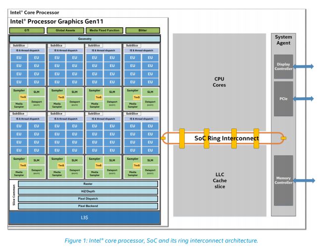
As we can see above in the basic block diagram of an Ice Lake processor, Intel's SoC (System On a Chip) design, which is used in its Core series of processors, is connected via a ring interconnect that ties together the CPU cores, GPU cores, LLC (Last Level Cache), and the system agent functions (PCIe, memory and display controllers). This arrangement confirms that Intel will use a ring bus interconnect for connecting the different chip structures.
Notably, the last level cache (LLC) is shared between both the CPU cores and the graphics, which eliminates data movement too and from the respective units. The SoC design has numerous clock domains split out into per-CPU core, processor graphics clock, and ring interconnect clock domains.
Get Tom's Hardware's best news and in-depth reviews, straight to your inbox.
The engine features support for tile-based rendering in addition to immediate mode rendering, which helps to reduce memory demands during some rendering workloads.
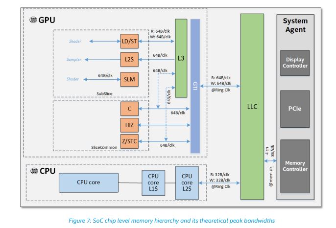
Here we see a birds-eye view of the memory hierarchy and the associated theoretical peak bandwidths between the components. Intel's move to support for LPDDR4 represents a significant step forward in bandwidth on the low-power front, but the true innovation lies in the shared memory design that reduces the need for copying data through buffers.
The GTI (Graphics Technology Interface) connects the GPU to the rest of the SoC, like the LLC memory and DRAM, and Intel improved performance from 32B/clock to 64B/clock for write operations, along with refining the internal queues to improve latency and bandwidth. Here we can see that the GPU can read and write to the ring at 64B/clock, while the CPU can only read and write at 32B/clock, meaning the GPU has a faster pathway to the shared last level cache (L3) at its disposal. In addition, the GPU has its own dedicated 3MB internal L3 cache that serves as an intermediary between the subslices and GTI.
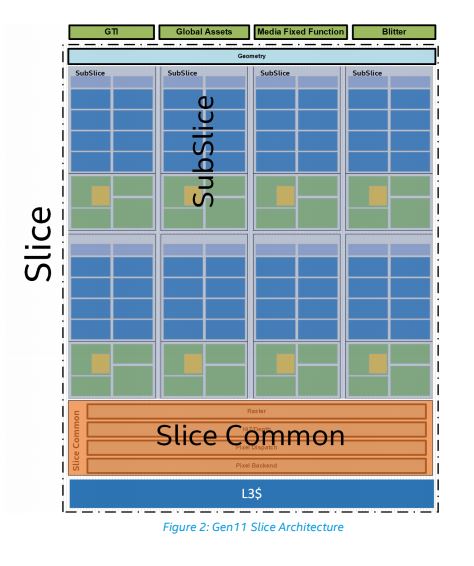
Each slice houses 3D Fixed Function Geometry, eight sub-slices containing the EUs, and a "slice common" that holds various fixed function blocks and writes to the slice's L3 cache. Intel improved the memory subsystem by quadrupling the L3 cache to 3MB and separated the shared local memory to promote parallelism. The new design also has enhanced memory compression algorithms.
Other improvements include a new HEVC Quick Sync Video engine that provides up to a 30% bitrate reduction over Gen9 (at the same or better visual quality), support for multiple 4K and 8K video streams within a lower power envelope, and support for Adaptive Sync technology. VP9 decode bit depth is improved up to 10 bits (from 8) to support HDR video.
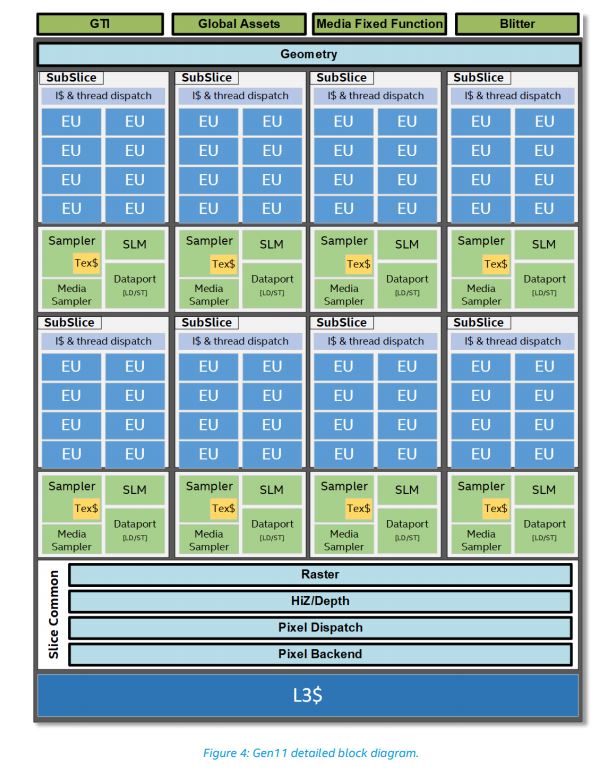
Diving deeper down into the slice, we can see that each slice houses eight subslices, each with eight EU. Each subslice houses a local thread dispatcher unit and its own instruction caches to feed it. A shared local memory (SLM), 3D texture sampler unit, media sampler unit, and dataport unit round out each subslice.
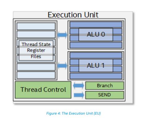
Focusing the microscope deeper into the multi-threaded execution unit (EU), we can see a pair of SIMD floating-point units (ALUs), but these units actually support both floating point and integer operations. Intel lists the ALUs (four execution pipelines apiece) as capable of executing four 32-bit FP or integer operations, or up to eight 16-bit FP operations. That equates to 16 FP32 operations per clock, or 32 FP16 operations per clock.
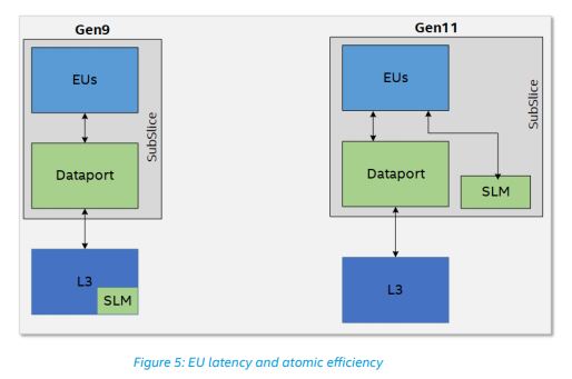
A closer look at the shared local memory (SLM) design, which feeds the eight EU in each subslice, reveals that Intel brought the SLM into the subslice to reduce contention through the dataport when the L3 cache is being simultaneously accessed. SLM's closer proximity to the EUs also helps reduce latency and boosts efficiency.
Image Credits: Intel

Paul Alcorn is the Editor-in-Chief for Tom's Hardware US. He also writes news and reviews on CPUs, storage, and enterprise hardware.
