Nvidia Patents Face-to-Face 3D Stacked Dies for its Future GPUs
Another approach to 3D packaged processors

Get Tom's Hardware's best news and in-depth reviews, straight to your inbox.
You are now subscribed
Your newsletter sign-up was successful
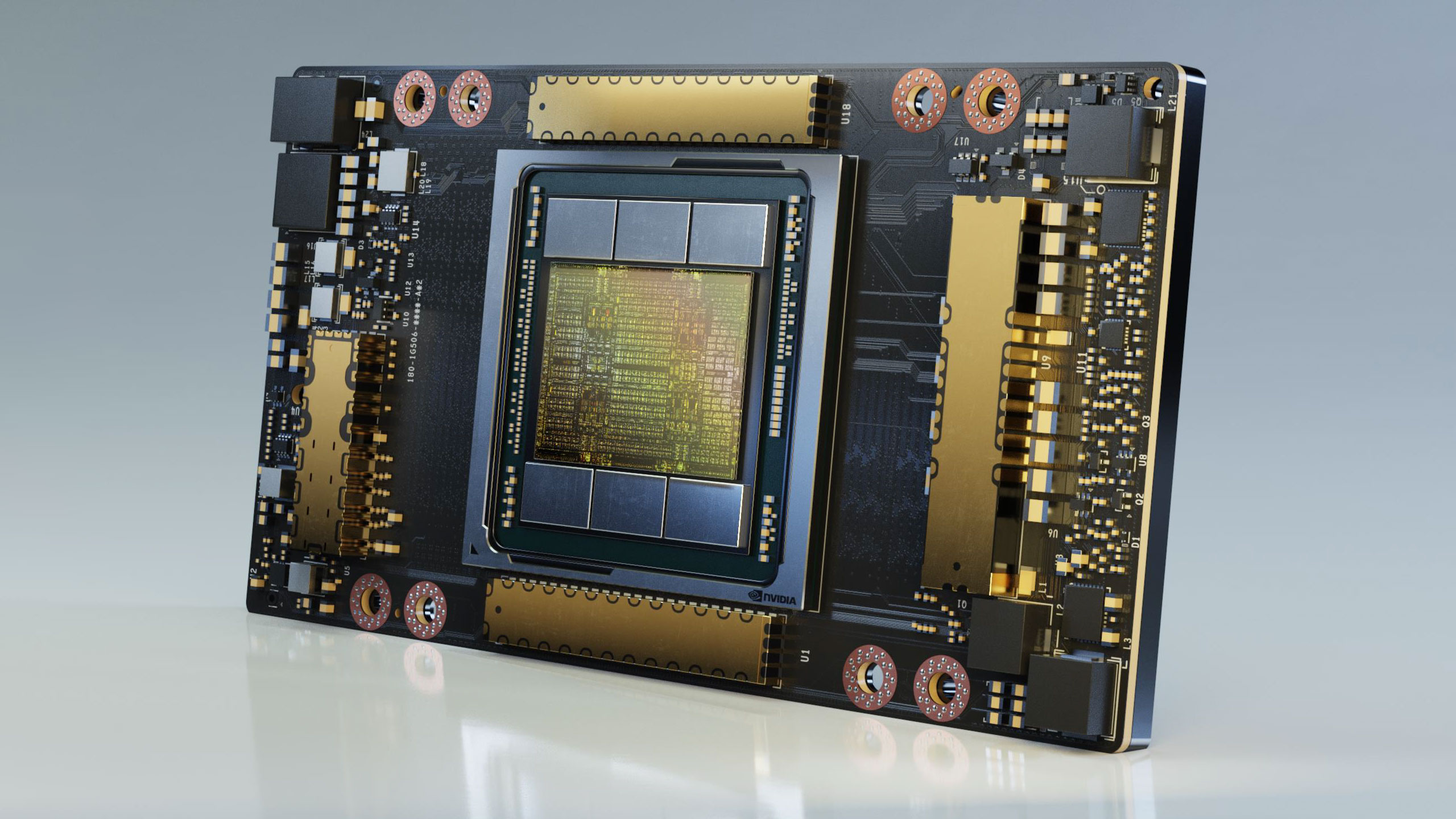
Semiconductor companies have been exploring ways to step out of the traditional monolithic GPU die design for a while now, searching for something that will enable better performance scaling while keeping production costs at a sane level. Nvidia's latest approach to driving things forward is the introduction of 3D die stacking using through-silicon via (TSV) technology with an enhanced power delivery approach. This sounds similar to technology we've already heard about from AMD, Intel, and TSMC, but there are some differences.
We already know that Nvidia has been planning to move away from monolithic die design. The company has been actively exploring ways of getting more performance using different packaging techniques, the most recent being the use of multi-chip modules (MCM) to build GPUs with continued performance scalability.
Back in 2017, Nvidia presented its MCM-GPU design at the International Symposium on Computer Architecture (ISCA). Nvidia planned to use multiple dies of logic to interconnect the massive amount of cores and develop new GPUs with continuous performance improvement while managing costs. As GPU dies get bigger, their costs increase exponentially, so making a few interconnected smaller dies is a more cost-effective solution. The MCM-GPU packaging approach solves this as it connects multiple dies that provide a huge performance uplift in return.
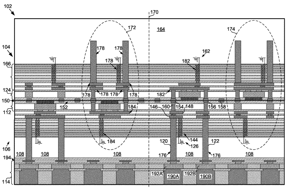
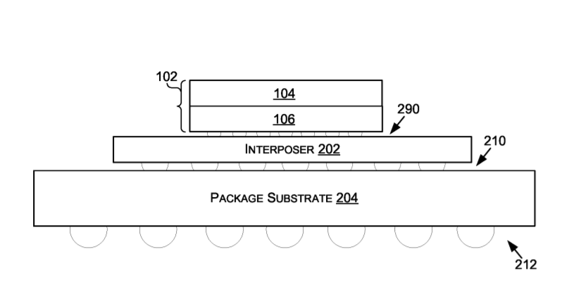
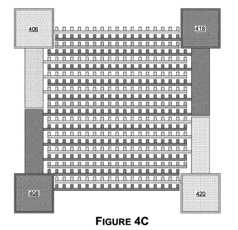
Article continues belowChip design isn't restricted to two dimensional scaling, and that's what Nvidia has patented today. Called "Face-to-face dies with enhanced power delivery using extended TSVs," Nvidia proposes the 3D stacking of semiconductor dies with a special note on enhanced power delivery using extra-long through-silicon vias (TSVs).


The way this setup works is that the base die is first tested using probe pads on the face of the die. After that, an interface layer is formed on the face of the first die, laid over the probe pads already present. Finally, the second die is taken and mounted over the interface layer, connecting the pads of the inter-die interface to the complementing connection on the other dies. This creates a face-to-face mounting of the dies and the 3D chip is born.
Nvidia's patent focuses on enhanced power delivery using extra-long TSVs. When stacking dies on top of each other like this, you can connect anything from logic (processing cores) to memory. Usually, connecting memory doesn't require much power, so the mention of enhanced power delivery leads us to conclude that Nvidia plans to perform stacking of processing cores, creating a computation-oriented approach to 3D processors.
Of course, the application for a patent doesn't mean actual products have to use the patented technology. Companies often patent inventions to prevent others from doing so, or just as a placeholder for future products. In either case, we already know that the MCM-GPU approach is coming, and some of the next-generation GPU architectures like Hopper could utilize the benefits of 3D die stacking to gain a competitive advantage.
Get Tom's Hardware's best news and in-depth reviews, straight to your inbox.
-
rubix_1011 THIS IS SUCH GREAT NEWS!Reply
Now tell me how they plan to reduce over-pricing of GPUs while also making them readily accessible without shortage. I think we're all really wondering how they can solve those problems first.
Otherwise, this is just more of the same - 'New, high-end GPU will be available in 202x....' but no one can buy it because of <insert shortage reason here>.
We keep hearing about flying cars, time travel and magic, although we at least have a realistic understanding from the marketing of those items.