Nvidia Submits First Grace Hopper CPU Superchip Benchmarks to MLPerf
Nvidia submits its first MLPerf scores for its homegrown CPU+GPU and its L4 GPUs.
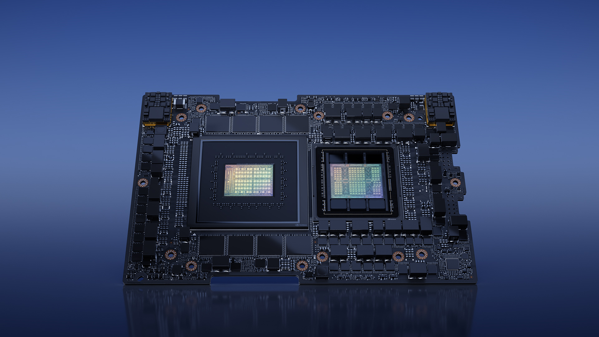
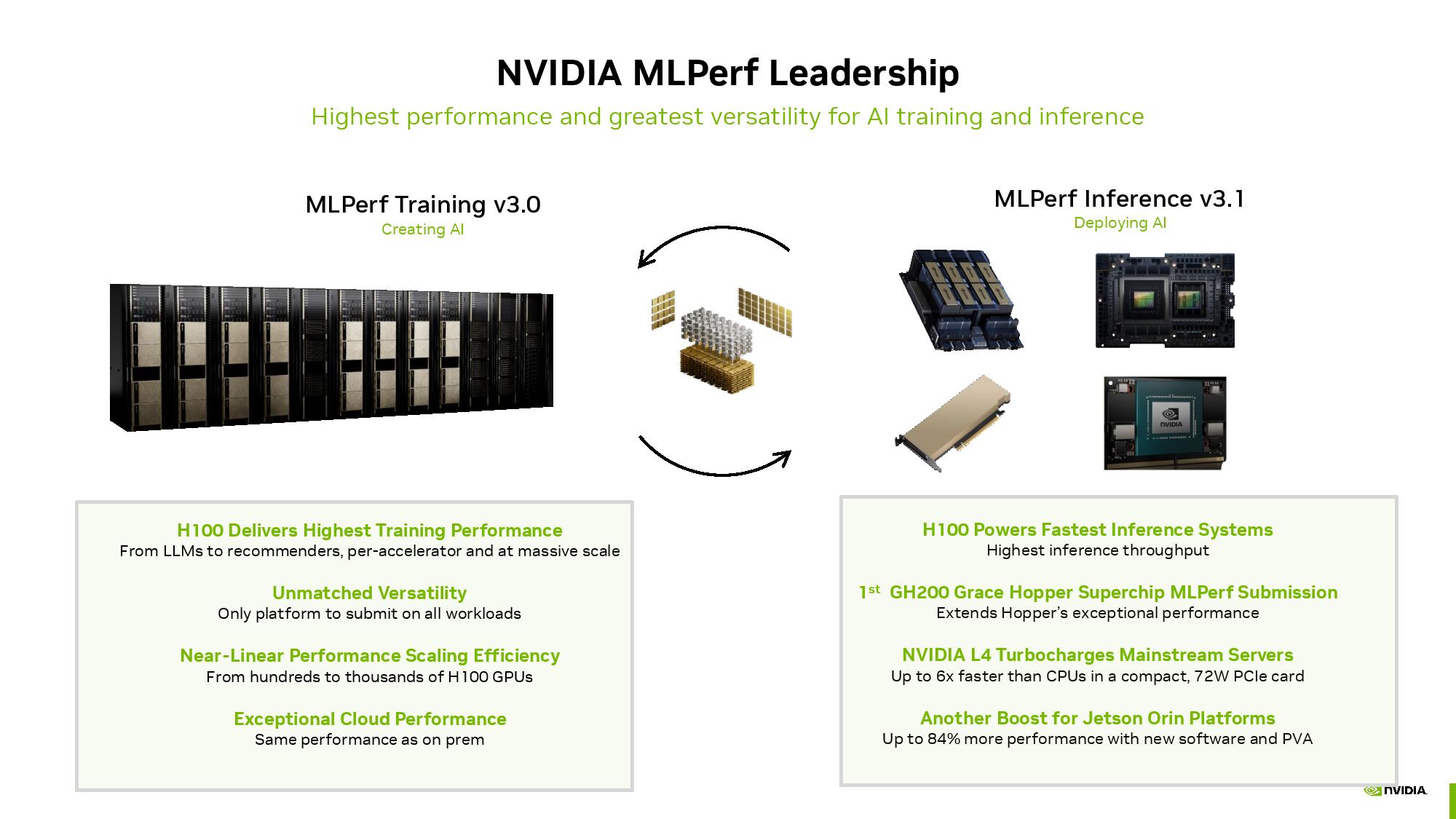
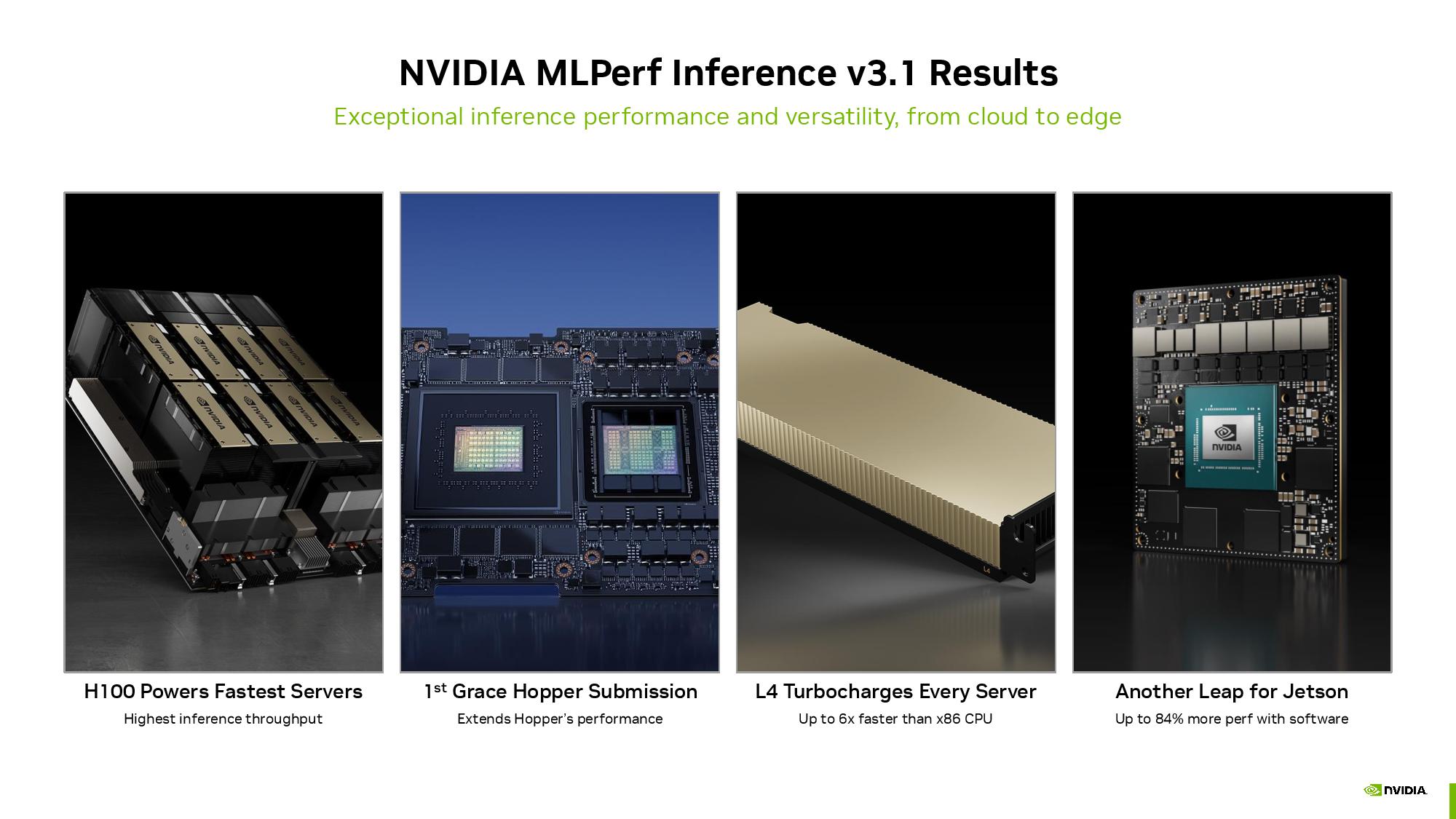
Nvidia announced today that it had submitted its first benchmark results for its Grace Hopper CPU+GPU Superchip and its L4 GPU accelerators to the newest version of MLPerf, an industry-standard AI benchmark that's designed to offer a level playing field for measuring AI performance in different workloads. Today's round of benchmark results marks two notable new firsts for the MLPerf benchmark: The addition of a new Large Language model (LLM) GPT-J inference benchmark and a revamped recommendation model. Nvidia claims the Grace Hopper Superchip delivers up to 17% more inference performance than one of its market-leading H100 GPUs in the GPT-J benchmark and that its L4 GPUs deliver up to 6X the performance of Intel's Xeon CPUs.
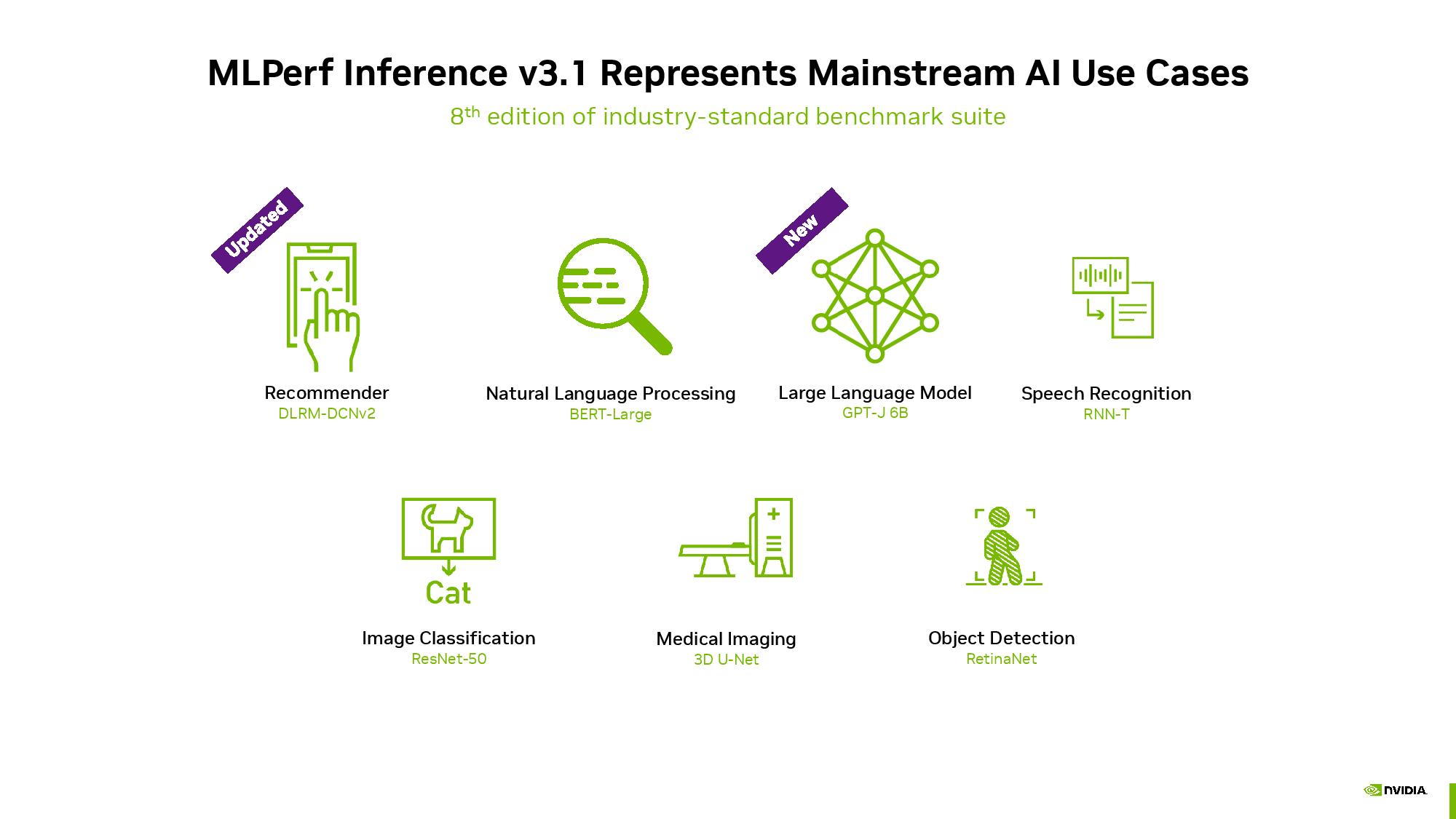
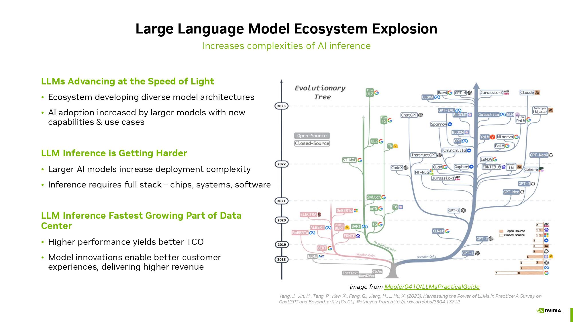
The industry is moving at breakneck speed as it rapidly evolves to newer AI models and more powerful implementations. In the same vein, the MLPerf benchmark, managed by the MLCommons body, is constantly evolving to better reflect the changing nature of the AI landscape with its new v3.1 revision.
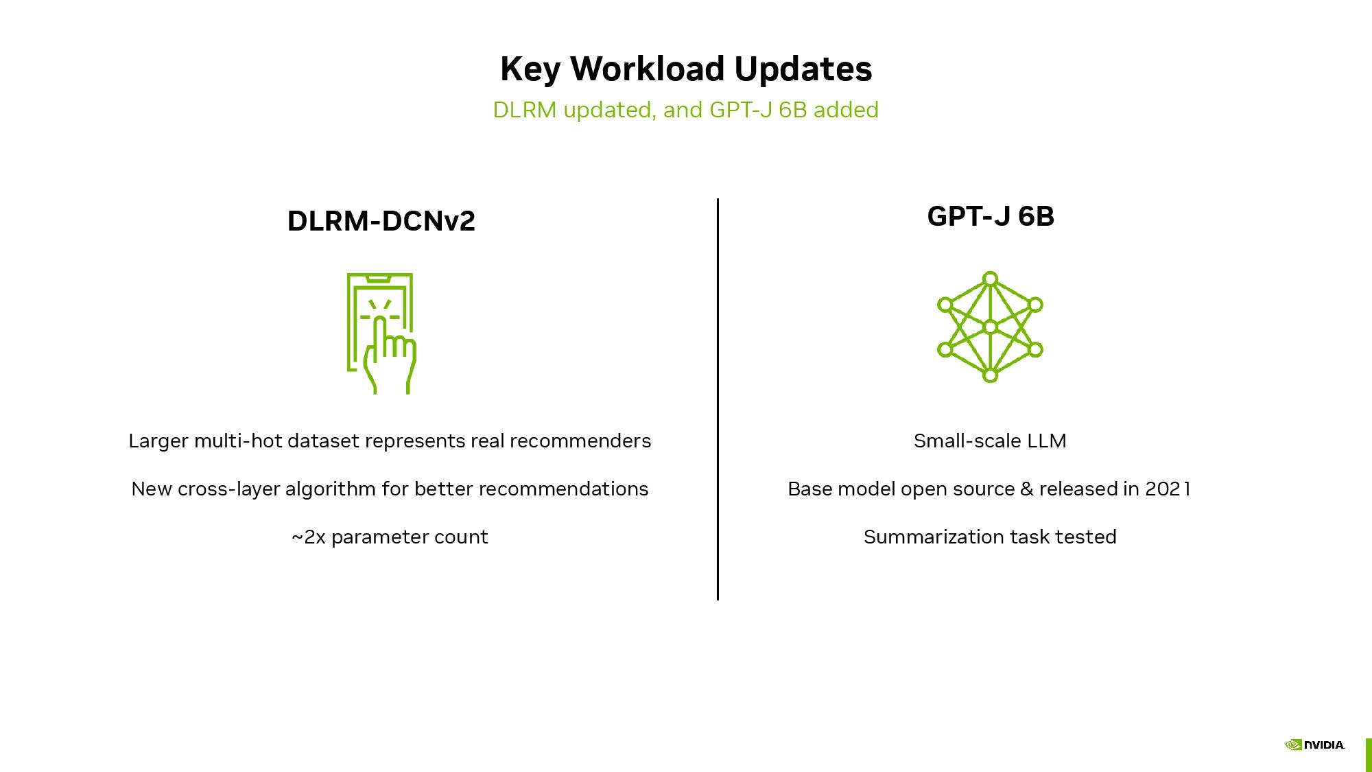
GPT-J 6B, a summarization model for text used in real-world workloads since 2021, is now used within the MLPerf suite as a benchmark for measuring inference performance. The GPT-J 6-billion-parameter LLM is rather lightweight compared to some of the more advanced AI models, like the 175-billion-parameter GPT-3, but it fits the role of an inference benchmark nicely. This model summarizes blocks of text and operates in both online mode, which is latency sensitive, and offline mode, which is throughput-intensive. The MLPerf suite also now employs a larger DLRM-DCNv2 recommendation model with twice the parameter count, a larger multi-hot dataset, and a cross-layer algorithm that better represents real-world environments.
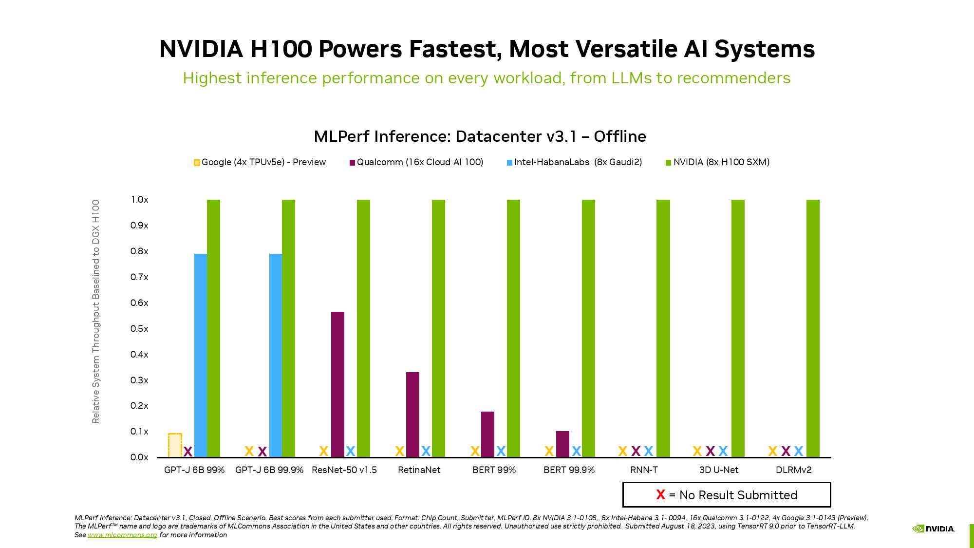

With that background, we can see some of Nvidia's performance claims here. Be aware that Nvidia itself submits these benchmarks to MLCommons, so they likely represent highly tuned best-case scenarios. Nvidia also likes to point out that it is the only company to submit benchmarks for every AI model used in the MLPerf suite, which is an objectively true statement. Some companies are wholly absent, like AMD, or only submit a few chosen benchmarks, like Intel with Habana and Google with its TPU. Reasons for the lack of submissions vary by company, but seeing more competitors step into the MLPerf ring would be nice.
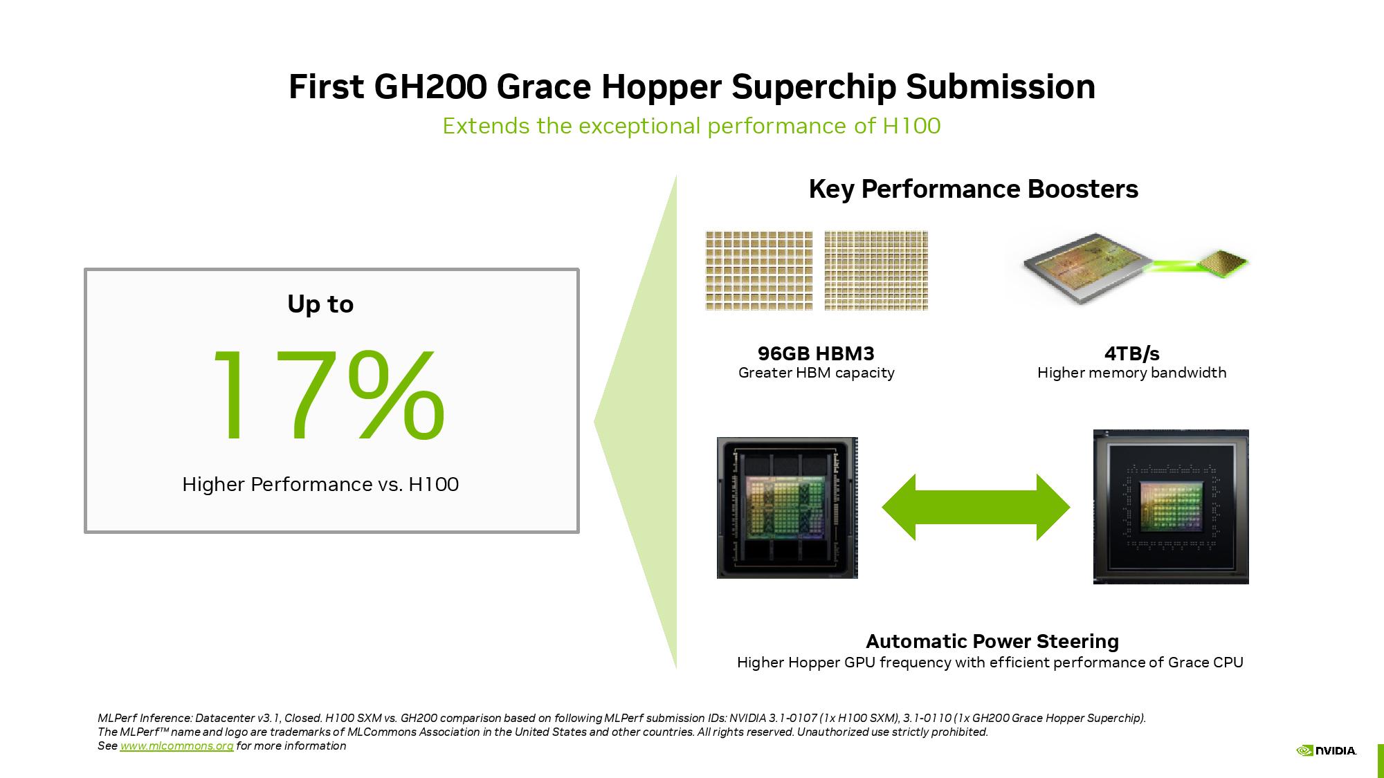
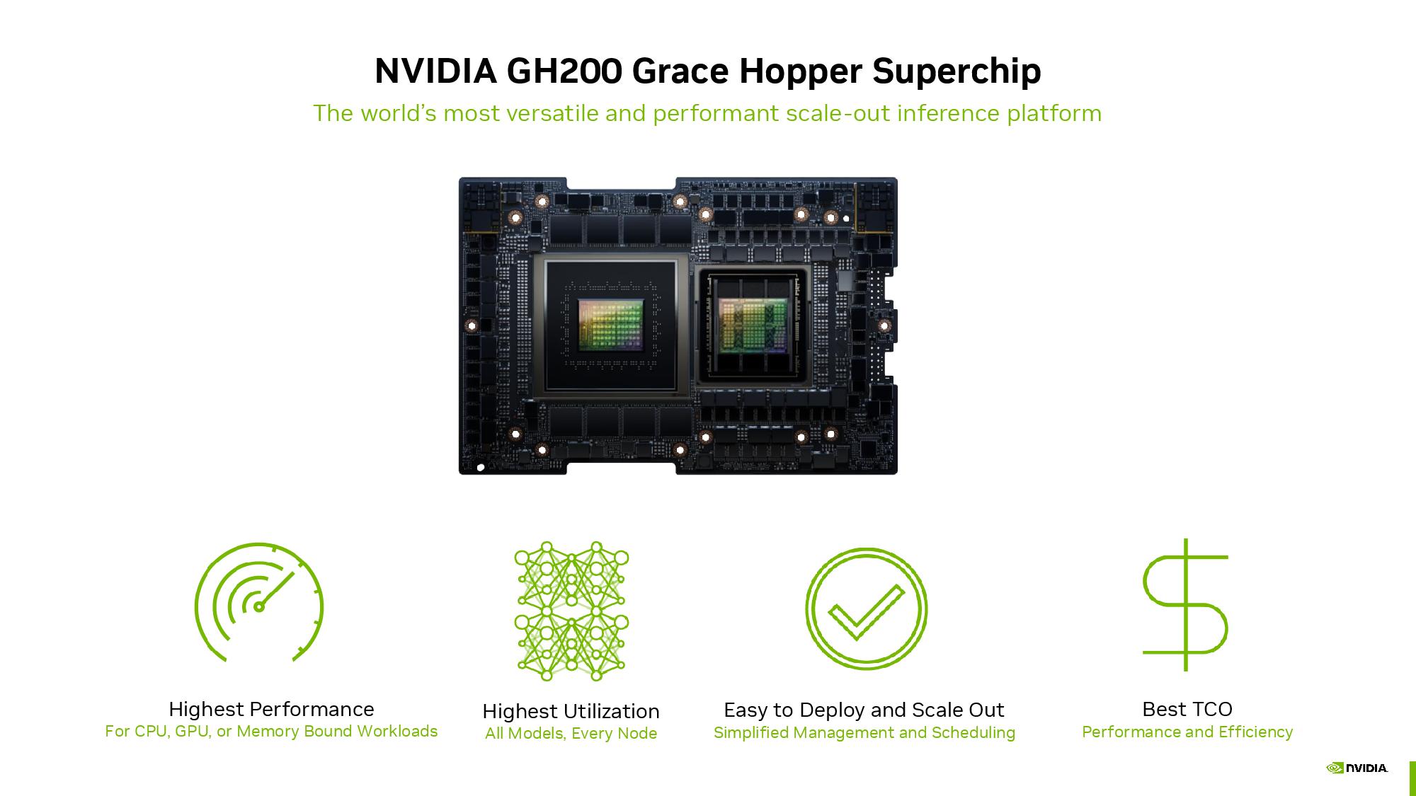
Nvidia submitted its first GH200 Grace Hopper Superchip MLPerf result, highlighting that the CPU+GPU combo delivers 17% more performance than a single H100 GPU. On the surface, that's surprising, given that the GH200 uses the same silicon as the H100 CPU, but we'll explain why below. Naturally, Nvidia's systems armed with eight H100s outperformed the Grace Hopper Superchip, taking the lead in every inference test.
As a reminder, the Grace Hopper Superchip combines a Hopper GPU and the Grace CPU on the same board, providing a C2C link (deep dive here) with 900GB/s of throughput between the two units, thus providing 7x the bandwidth of a typical PCIe connection for CPU-to-GPU data transfers, boosting the GH200's accessible memory bandwidth, augmented by a coherent memory pool that includes 96GB of HBM3 memory and 4TB/s of GPU memory bandwidth. In contrast, the comparison H100 tested in the HGX has only 80GB of HBM3 (next-gen Grace Hopper models will have 144GB of 1.7X faster HBM3e in Q2 2024).
Nvidia also touts a dynamic power-shifting tech called Automatic Power Steering that dynamically balances the power budget between the CPU and GPU, steering the spillover budget to whichever unit is under the most load. This tech is used in many competing modern CPU+GPU combos, so it isn't new, but it does allow the GPU onboard the Grace Hopper Superchip to enjoy a higher power delivery budget than it does in the HGX due to power being shifted from the Grace CPU — that isn't possible in a standard server. The full CPU+GPU system ran at a 1000W TDP.
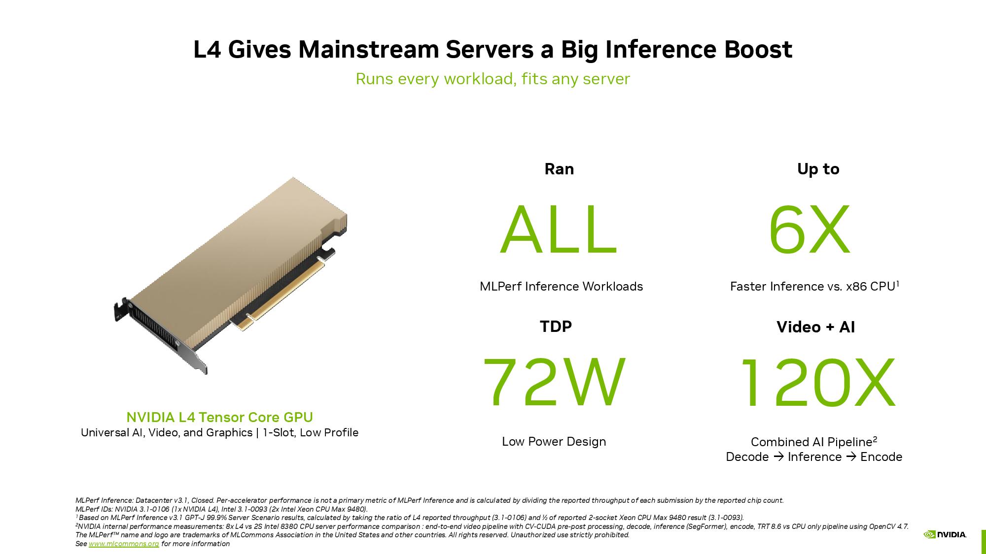
Most inference continues to execute on CPUs, which could change in the future as larger models become more common; Displacing CPUs for these workloads with small low-power GPUs like the L4 is paramount for Nvidia because it would fuel high-volume sales. This round of MLPerf submissions also includes the first results for Nvidia's L4 GPUs, with the inference-optimized card delivering 6X the performance of a single Xeon 9480 in the GPT-J inference benchmark, despite pulling a mere 72W in a slim form factor card that doesn't require an auxiliary power connection.
Nvidia also claims up to 120X the performance in a video+AI decode-inference-encode workload against CPUs by measuring the performance of eight L4 GPUs versus two previous-gen Xeon 8380s CPUs, which is a bit lopsided. This is probably intended to be a direct comparison of the sheer amount of computing power that can be crammed into a single chassis. Still, it's noteworthy that quad-socket servers are available despite not being the best fit for the job, and newer Xeon chips would probably perform a bit better in this test. The test configuration is in the small print at the bottom of the slide, so be sure to pay attention to those details.
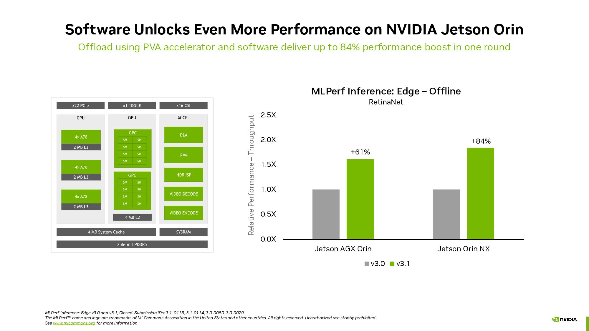
Finally, Nvidia also submitted benchmarks of its Jetson Orin robotics chips, showing an 84% gain in inference throughput that's largely driven by improvements to software.
Get Tom's Hardware's best news and in-depth reviews, straight to your inbox.
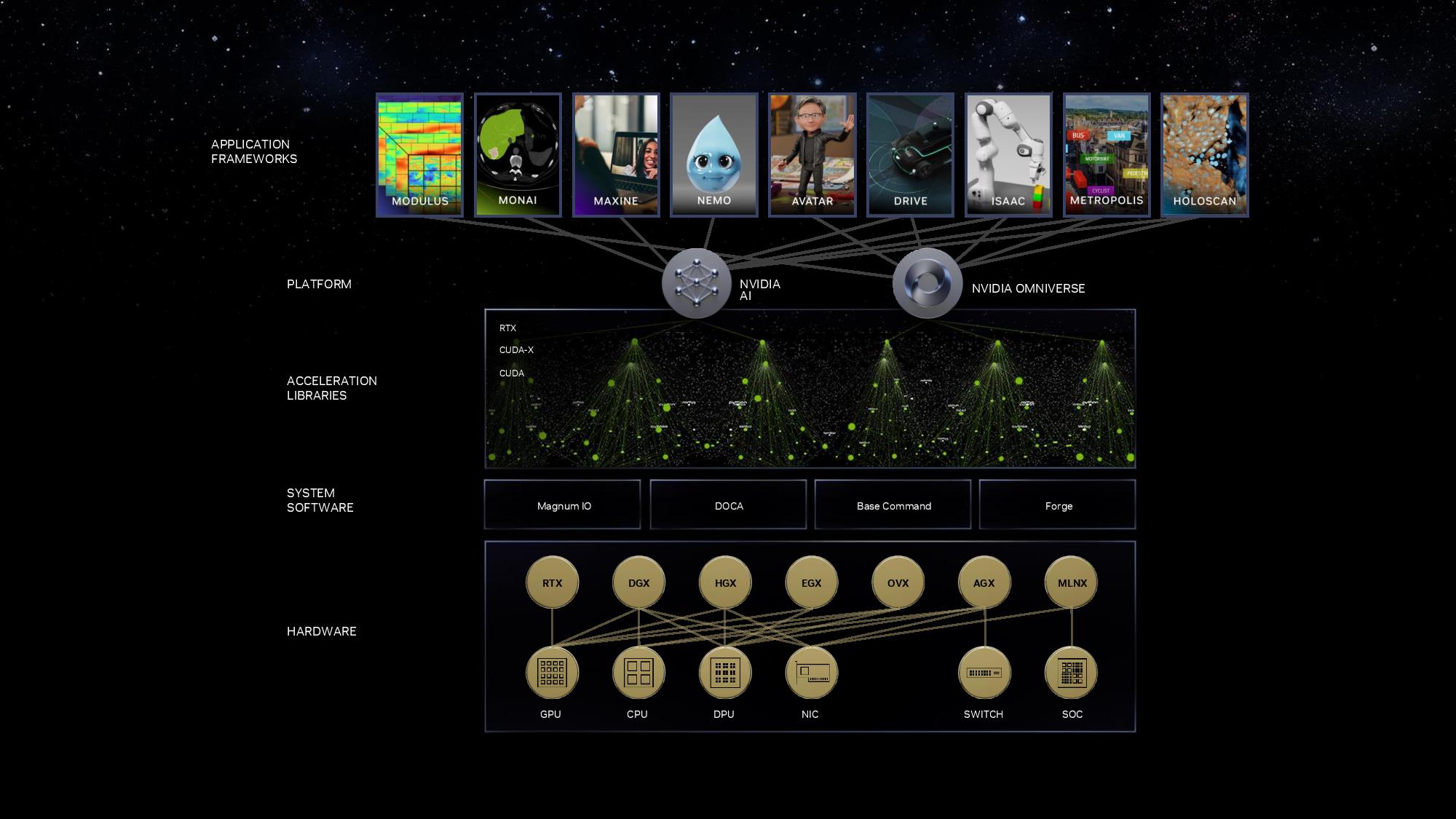

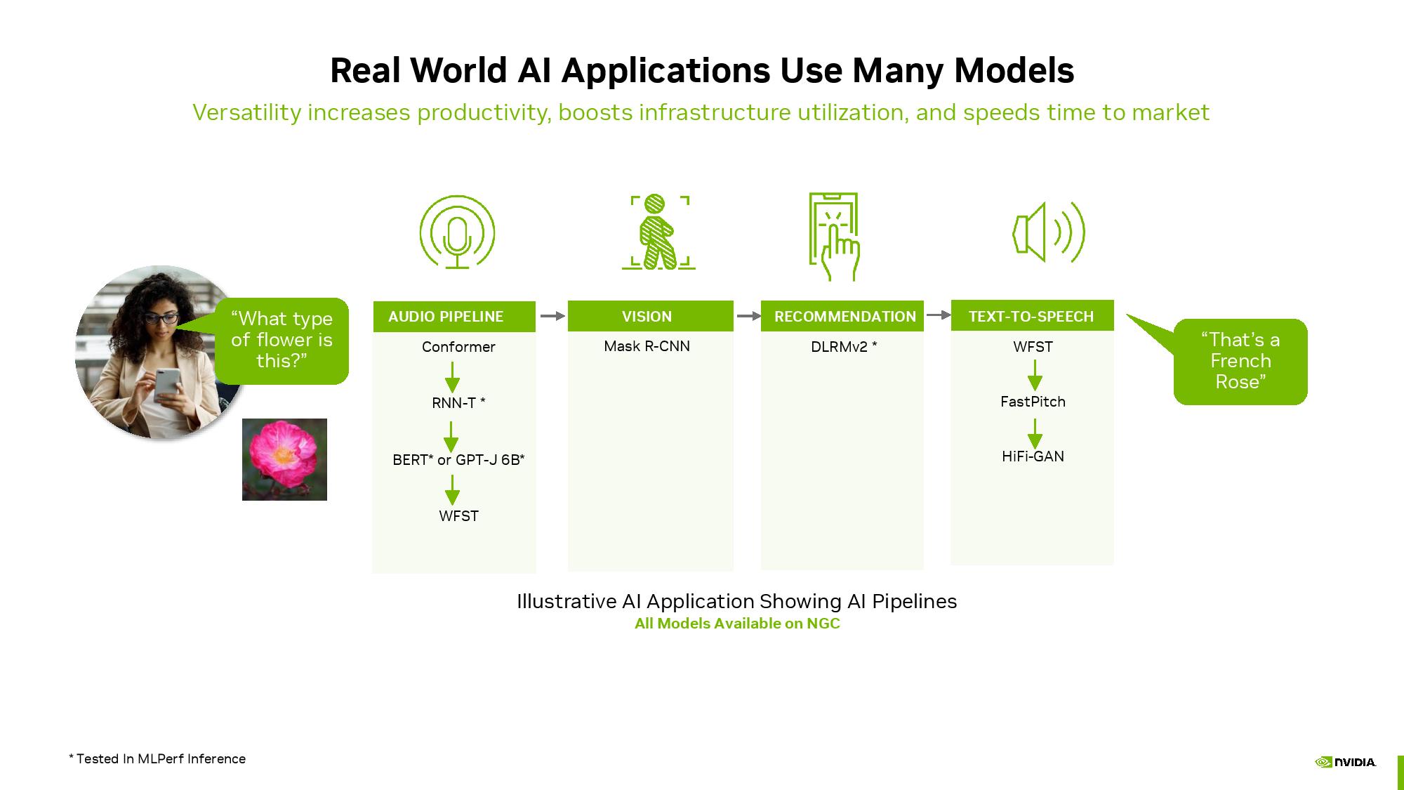
it's important to remember that, in the real world, each AI model runs as part of a longer series of models that execute in an AI pipeline to accomplish a specific job or task. Nvidia's illustration above encompasses this nicely, with eight different AI models being performed on one query before completion — and it isn't unheard of for these types of AI pipelines to extend up to 15 networks to satisfy a single query. This is important context, as the throughput-oriented benchmarks above tend to focus on running a single AI model at high utilization, as opposed to the real-world pipeline that requires quite a bit more versatility with multiple AI models running serially to complete a given task.
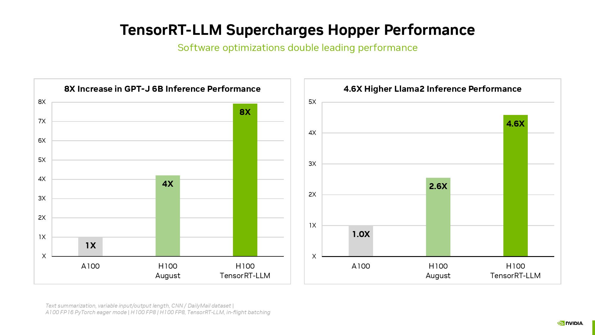
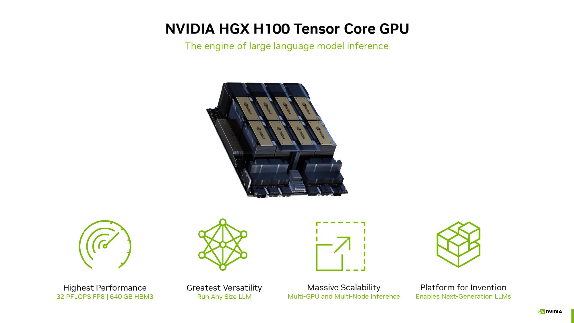
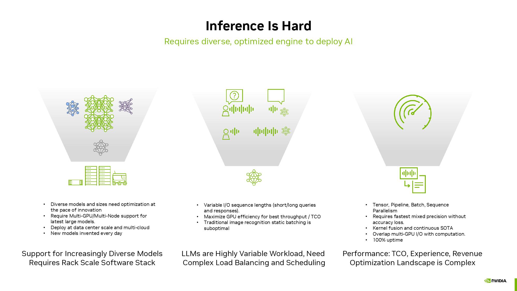
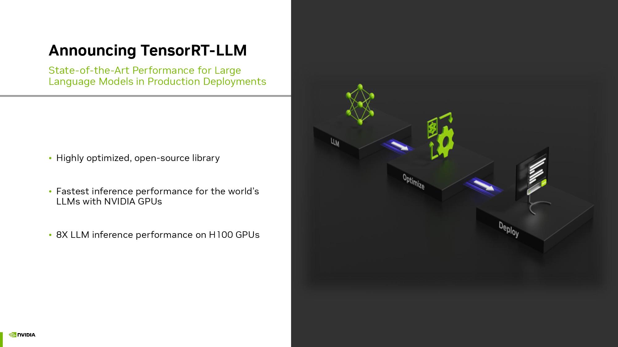
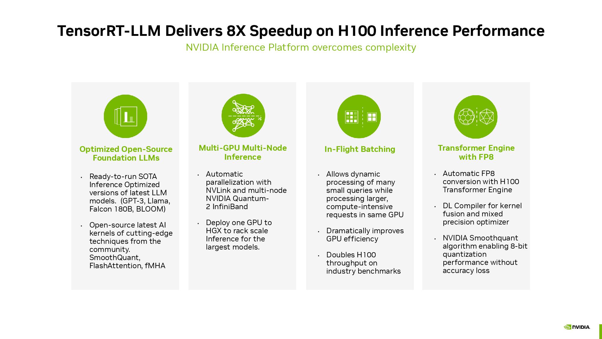
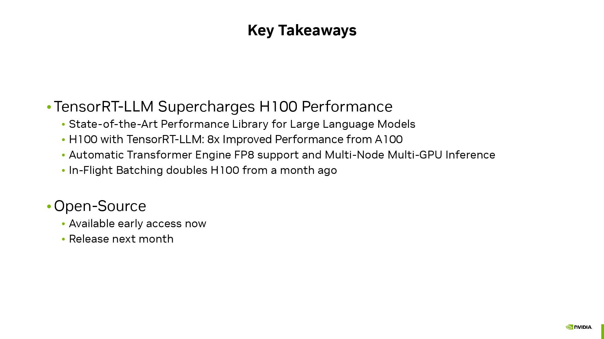
Nvidia also announced last week that its TensorRT-LLM software for generative AI workloads delivers optimized performance in inference workloads, overall delivering more than double the performance when used on its H100 GPUs, at no added cost. Nvidia provided details about this software recently, which you can read about here, and points out that it didn't have this inference-boosting software ready for this round of results; MLCommons requires a 30-day lead time for MLPerf submissions, and TensorRT-LLM wasn't available at the time. That means that Nvidia's inaugural round of MLPerf benchmarks should see a tremendous improvement with the next round of submissions.

Paul Alcorn is the Editor-in-Chief for Tom's Hardware US. He also writes news and reviews on CPUs, storage, and enterprise hardware.
-
artk2219 Reply
To be fair you do want to market your stuff to get sales. The other part of that is, I mean, of course they're full of themselves, it's Nvidia hah.NeoMorpheus said:They are really full of themselves even on the naming dept... -
bit_user Reply
It helps to understand what they mean by it. Although they don't shy away from making it sound like a superlative, they call it a "superchip" because it's actually a pair of chips. So, being more than a single chip - and yet it still behaves as a logical unit, in some respects - it's not technically incorrect to call it a "superchip".NeoMorpheus said:"Superchip"
They are really full of themselves even on the naming dept...
They support 3 different pairings:
Grace + Grace
Hopper + Hopper
Grace + Hopper
The entire pair fits on a single SXM daughter card. -
NeoMorpheus Reply
Soooo, just like all AMD APU's, SOC's and their MI300 chips?bit_user said:It helps to understand what they mean by it. Although they don't shy away from making it sound like a superlative, they call it a "superchip" because it's actually a pair of chips. So, being more than a single chip - and yet it still behaves as a logical unit, in some respects - it's not technically incorrect to call it a "superchip".
They support 3 different pairings:
Grace + Grace
Hopper + Hopper
Grace + Hopper
The entire pair fits on a single SXM daughter card.
Actually, AMD should then call the MI300X The UltraChip! (including the exclamation mark :-) ) given the monster that it claims to be. -
bit_user Reply
That's a different, because you can't have one of those chiplets in isolation. In Nvidia's case, we already have H100 GPUs on their own card and you could obviously do the same thing with a Grace CPU. So, it's not the same kind of arrangement.NeoMorpheus said:Soooo, just like all AMD APU's, SOC's and their MI300 chips?
What AMD's chiplet-based CPUs are classically called is a MCM (Multi-Chip Module).
Eh, I guess they can call it whatever they want.NeoMorpheus said:Actually, AMD should then call the MI300X The UltraChip! (including the exclamation mark :-) ) given the monster that it claims to be. -
TJ Hooker Yeah, the "superchip" sounds like something closer to a dual socket motherboard concept. I.e. two separate processor packages on a single board, both capable of independent operation, rather than multiple chiplets/tiles in a single package. Except it's different than a dual socket motherboard, in that both processors can either a CPU or GPU, among other things.Reply -
bit_user Reply
There's an important distinction, here. It's not like just having a dual-socket motherboard, because these Superchips typically exist as nodes in the context of a larger, cache-coherent system with a unified memory space. You can have like 8 or maybe more of these nodes sharing the same memory space, connected via NVLink.TJ Hooker said:Yeah, the "superchip" sounds like something closer to a dual socket motherboard concept. I.e. two separate processor packages on a single board, both capable of independent operation, rather than multiple chiplets/tiles in a single package.
It's worth pointing out that the main advantage Nvidia gets from these Grace + Hopper superchips is that the Grace nodes let them intersperse 512 GB of memory throughout the NVLink topology. This gives them scalable, distributed memory to help support the Hopper GPUs.
Say what you want about their business practices, but Nvidia knows what it's doing, engineering-wise. No matter what their business practices, they couldn't maintain their lead, in this hyper-competitive industry, without the top engineering talent to back it up. -
NeoMorpheus Reply
Wouldn that apply with Ryzen Z1/Extreme and SOCs in the last couple of consoles?bit_user said:That's a different, because you can't have one of those chiplets in isolation. In Nvidia's case, we already have H100 GPUs on their own card and you could obviously do the same thing with a Grace CPU. So, it's not the same kind of arrangement.
What AMD's chiplet-based CPUs are classically called is a MCM (Multi-Chip Module).
Because last I checked, they are all one chip, not MCM, but I could be wrong.
Given how things are going, we should trive for more silly names :-Dbit_user said:Eh, I guess they can call it whatever they want.