Quad-Layer 3D Wafer Stacking Technology Enables Chips of the Future
A veritable wafer sandwich is now possible.

True next-gen 3D chip stacking may be right around the corner, as researches from the Institute of Microeletronics (IME) have just achieved a technology breakthrough that enables up to four semiconductor layers to be stacked. This enables up to 50% savings compared to traditional 2D fabrication techniques, and the technique will likely be used in the best CPUs and best graphics cards of the future.
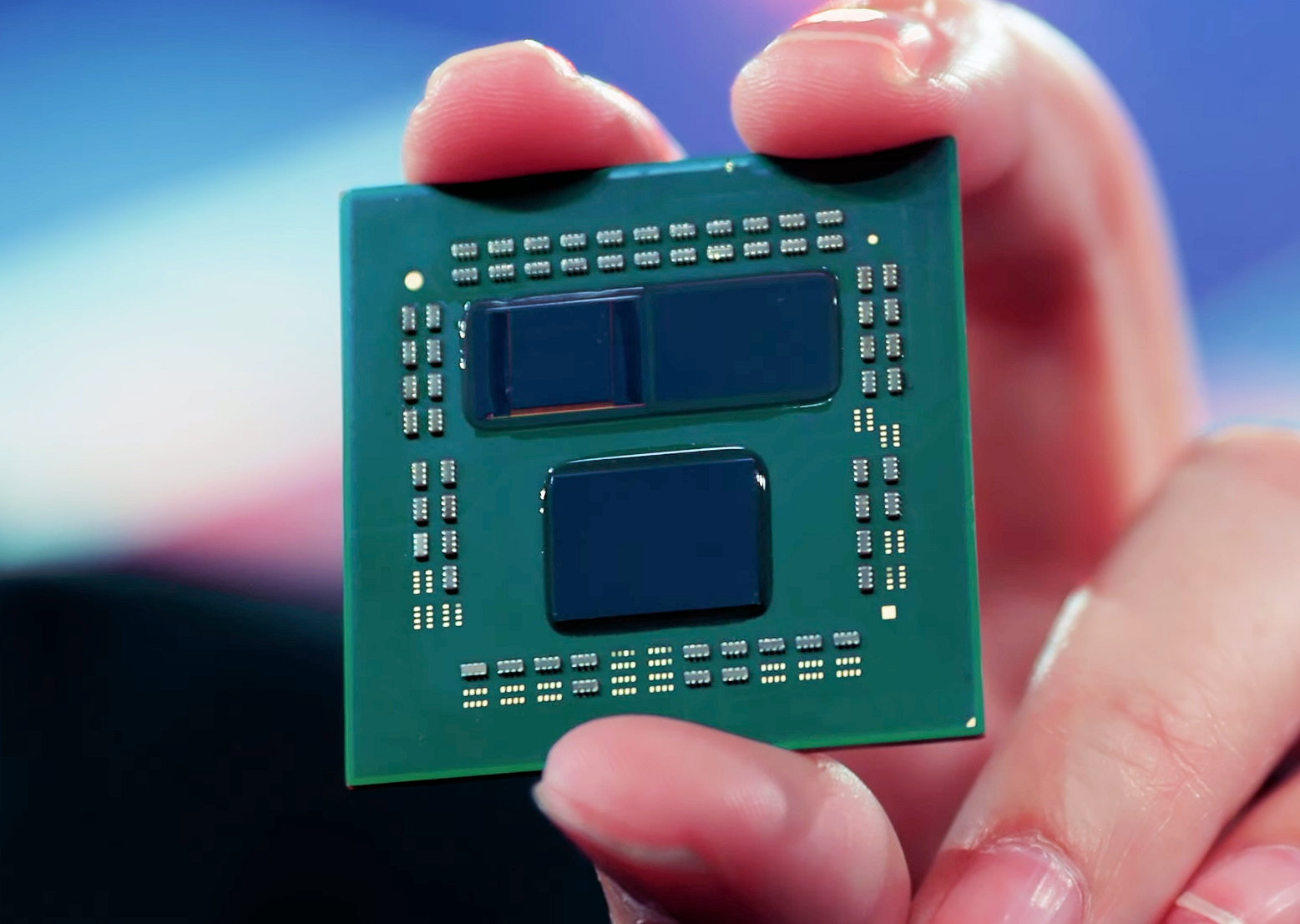
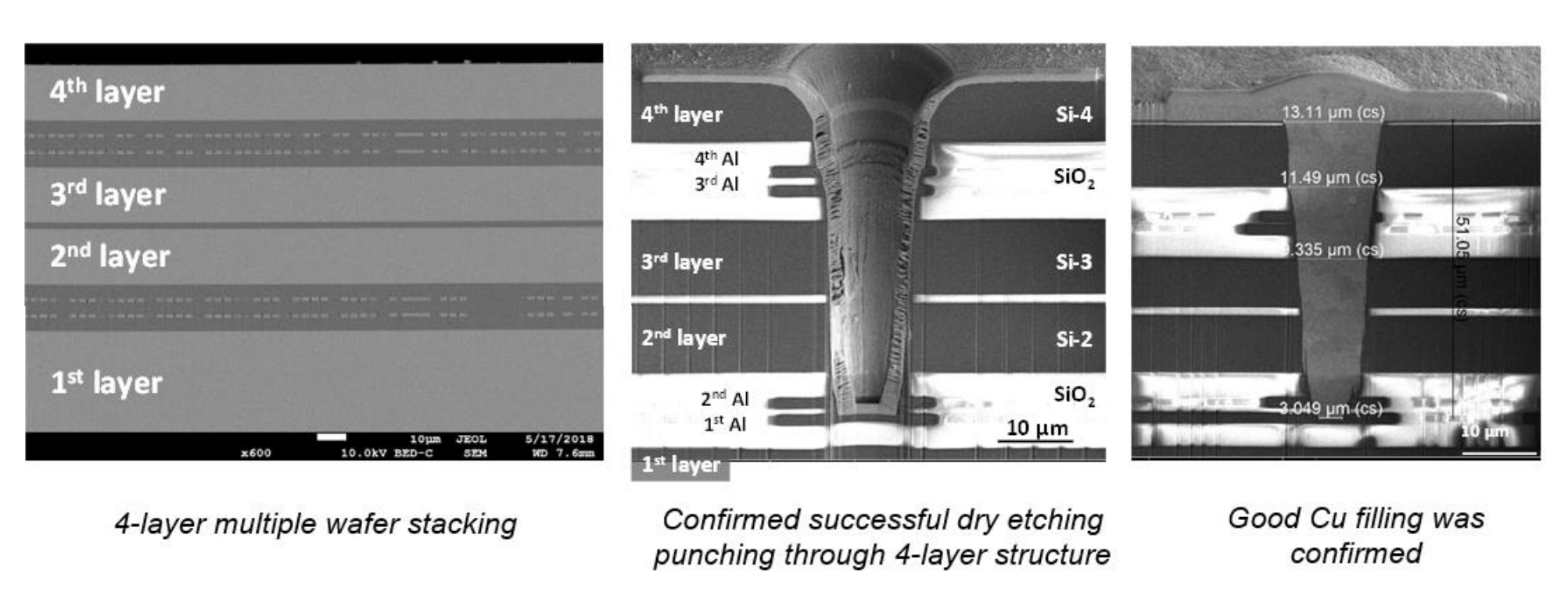
This achievement is a step-up from the AMD-announced, TSMC-enabled SRAM stacking that's bound to grace our computers by the end of this year, as that particular process currently only enables two dies (in AMD's case, a Zen 3 CCX on layer one and 96MB of SRAM cache on layer two) to be bonded together. The IME researchers have shown a process where they successfully bonded four separate silicon layers via TSVs (Through-Silicon-Vias), the information highways allowing communication between the different dies.

TSVs and the active wafer stacking they enable are hailed as one of the most important technological breakthroughs for sustaining (and perhaps even improving upon) Moore's Law, since they allow for wider information buses that need not operate at extremely high frequencies to achieve performance goals. This, in turn, enables denser designs, since some components that were previously arranged horizontally can now be vertically stacked. It also allows for higher power efficiency, more efficient heat dissipation, and even offers improvements do yields. That last is because different components that go into a CPU, for instance, can now be manufactured in different wafers instead of the old, monolithic approach, automatically increasing resilience to manufacturing defects.
Article continues below 
The manufacturing approach implemented by IME was achieved "...by combining Face-to-Face and Back-to-Back wafer bonding with onestep TSV after stacking." This means that the first, base layer has its "face" towards the second layer, which is also facing it; and the second layer has its "back" towards the third layer's back, which in turn faces the fourth layer's face. After these layers were bonded, IME then proceeded to "punch" them by etching along specifically-designed pathways that finally become the TSVs through which data flows.
If you're thinking that increased verticality should wreak havoc with temperature dissipation despite efficiency gains, you're right. That's why (currently) exotic, direct-to-die cooling technologies are being developed as we speak. Data cubes will soon become more than just science fiction.
Get Tom's Hardware's best news and in-depth reviews, straight to your inbox.

Francisco Pires is a freelance news writer for Tom's Hardware with a soft side for quantum computing.
-
Kamen Rider Blade What happens if you have cooling on both sides of the PCB / Direct Die contact?Reply
Would that help? -
I imagine the internal cooling will be closed loop with heat exchange pipes under cooler. It's going to make the CPU fragile. I wonder how will it be secured from accidental damage.Reply
-
drajitsh Could you please add a clarification as to how this will is different from HBM --as the HBM 1 in Fiji in 2015 had 4-hi memory+buffer logic+ interposerReply
https://www.tomshardware.com/news/amd-high-bandwidth-memory,29116.html -
hotaru.hino Reply
It's probably no different, maybe with the exception of one or two minor details.drajitsh said:Could you please add a clarification as to how this will is different from HBM --as the HBM 1 in Fiji in 2015 had 4-hi memory+buffer logic+ interposer
https://www.tomshardware.com/news/amd-high-bandwidth-memory,29116.html
This type of IC manufacturing has been around for a while too: https://www.researchgate.net/publication/271453642_3D_ICs_in_the_real_world -
TJ Hooker Reply
Can you elaborate on how memory stacking is fundamentally different than logic stacking?Francisco Alexandre Pires said:And memory layering works very, very differently from logic layering. -
drajitsh Reply
4 Zen or any compute dies attached on each other seems more of a technology demonstrator and any real world use, given thermal limitsFrancisco Alexandre Pires said:It's different because we're talking about four active silicon dies (that can be logic, SRAM, four Zen 3 dies, etc) being sandwiched together and connected directly via TSVs. An interposer isn't an active computing element (it's just a communications layer), so it doesn't count as one of these layers. And memory layering works very, very differently from logic layering.
The news here is that never before had a four-layer chip was actually manufactured.