Raja Koduri Flashes 'Petaflops Scale' GPU, 4-Tile Xe HP at Hot Chips
Proof that the massive package exists
Over the past several months, Intel's Raja Koduri has been slowly revealing portions of the upcoming Xe Graphics architecture and lineup. The Xe family will span everything from low power integrated and entry level graphics solutions under the Xe LP Graphics brand, up through data center multi-chip solutions with die stacking. The latter is we're talking about.
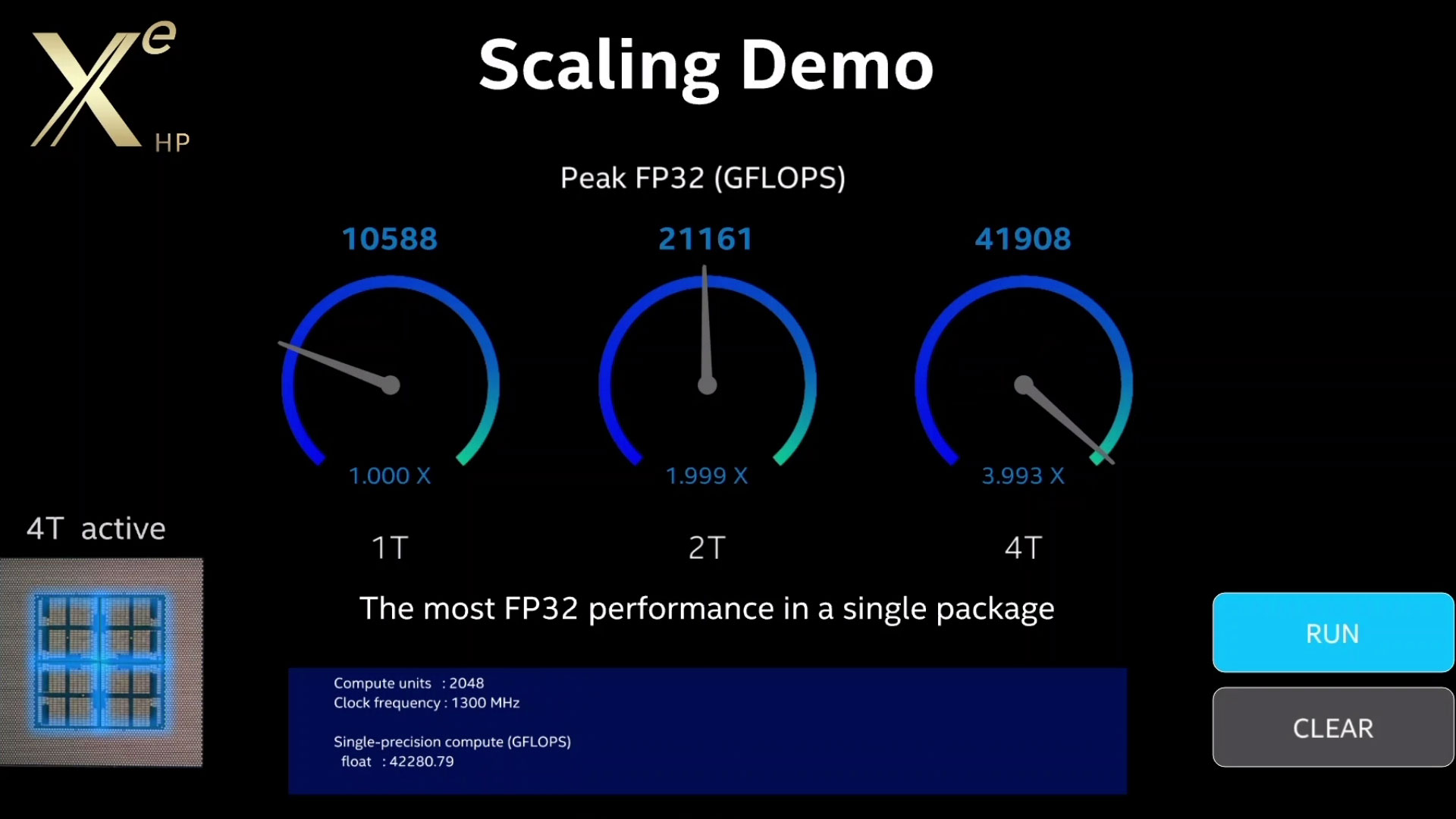
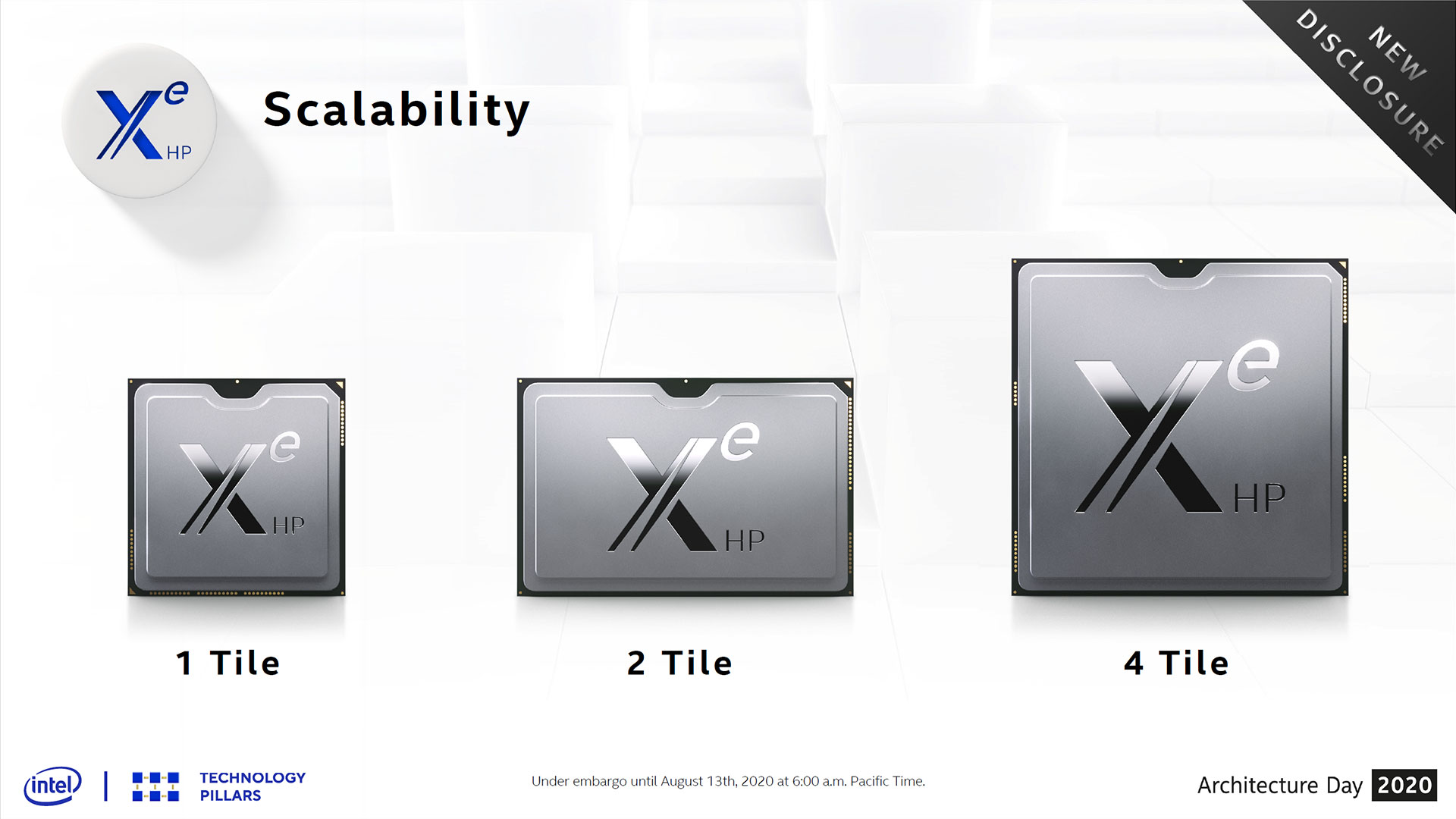
As discussed last week, Intel's Xe HP Graphics will come in three variants. The base model, which has been shown several times, has a single tile with 512 EUs (Execution Units) and most likely two HMB2e stacks. Intel hasn't confirmed exact specs, but it did show performance scaling for a computational workload of the 1-tile, 2-tile, and 4-tile variants:
The scaling from the additional tiles might look almost too perfect, but it's important to note that this is not a real-time graphics workload. Splitting work between GPUs for technologies like SLI and CrossFire is far more difficult to do and scaling from additional GPUs usually only nets gamers 50-80% more performance at best. For computational workloads, however, tasks are often independent and can thus hit perfect scaling.
Lest anyone doubt that the 4-tile GPU doesn't actually exist and is merely a publicity stunt, Raja whipped out the large package and briefly flashed it at the camera during his Hot Chips presentation. And yes, it's really big — much bigger than any other chip package we've seen.
Whether the 4-tile Xe HP will ever be put into production, or if it's merely a test product while Intel prepares Xe HPC, aka Ponte Vecchio, is a different matter.
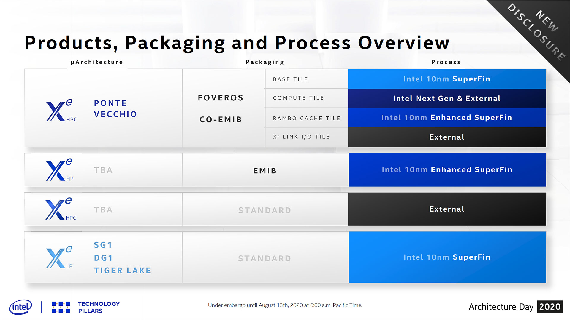
Xe HP only uses EMIB to scale to multi-tile configurations. Xe HPC will also include a Rambo Cache tile, Foveros die stacking, and Co-EMIB with additional enhancements. Ponte Vecchio is planned for use in the upcoming Aurora supercomputer, and it was supposed to be manufactured on Intel's now-delayed 7nm lithography.
In the meantime, Intel now has 1-tile, 2-tile, and 4-tile Xe HP silicon in its labs. As you'd expect, the EMIB linking means the packages for the latter two are basically 2x and 4x the size of the base design, so the GPUs require three separate sockets.
Get Tom's Hardware's best news and in-depth reviews, straight to your inbox.
The 4-tile implementation of Xe HP Raja showed off is capable of around 42 TFLOPS of FP32 compute. However, that's not actually the maximum capability. Raja also mentioned that the 4-tile chip is capable of reaching "petaflops scale computing," or >1000 TFLOPS. That's thanks to the presence of tensor cores, though we don't know the exact configuration.
Like Nvidia's A100 architecture and Google's TPUv4, Xe HP supports tensor cores. We assume these are capable of 128 operations per cycle, with one tensor core per EU. With 2048 EUs, that gives us:
2048 × 128 × 2 (FMA) = 524,288
We're missing clock speed, which would suggest either a 2GHz baseline for one petaflop, or potentially a different tensor core arrangement that can do more than 128 ops per clock. Either way, it should make it much easier for supercomputers to reach the level of exascale computing.

Jarred Walton is a senior editor at Tom's Hardware focusing on everything GPU. He has been working as a tech journalist since 2004, writing for AnandTech, Maximum PC, and PC Gamer. From the first S3 Virge '3D decelerators' to today's GPUs, Jarred keeps up with all the latest graphics trends and is the one to ask about game performance.
-
nofanneeded That guy worked for AMD as we know :)Reply
4 tiles ... wonderful , he is stealing AMD Technology in ThreadRipper/Epyc design ... I think AMD is waiting for the Release , and then "Court Time" ... -
JayNor David Blythe presented a chart that showed GPU clock speeds can approach 1.7GHz at high end of voltage range of the SuperFin process.Reply -
JayNor The CC info was that the CPUs planned for 7nm were delayed. The 7nm process was low yield. There was no mention of delaying the only 7nm GPU scheduled for 2021, which was Ponte Vecchio.Reply
btw, the HPG Xe chip which was listed as being fab'd externally was stated to be back in the lab already in David Blythe's presentation. Looks like this was not a last minute decision. They just didn't announce it. -
velocityg4 Replynofanneeded said:That guy worked for AMD as we know :)
4 tiles ... wonderful , he is stealing AMD Technology in ThreadRipper/Epyc design ... I think AMD is waiting for the Release , and then "Court Time" ...
Doesn't really matter. They'd fight it in court for many years as Intel rakes in the money. Then maybe get a billion dollar slap on the wrist. -
PapaCrazy Replynofanneeded said:That guy worked for AMD as we know :)
4 tiles ... wonderful , he is stealing AMD Technology in ThreadRipper/Epyc design ... I think AMD is waiting for the Release , and then "Court Time" ...
There's a difference between an idea and a technology. The first multi-core CPU was made by IBM, the first dual GPU made by 3DFX. Stacking silicon is not a new idea. -
vinay2070 Reply
AMD themselves dont have a tiled GPU yet. How can you be so sure the technology came from the CPU department of AMD when he was working on the GPU division? This might be a totally different design internally for all you know.nofanneeded said:That guy worked for AMD as we know :)
4 tiles ... wonderful , he is stealing AMD Technology in ThreadRipper/Epyc design ... I think AMD is waiting for the Release , and then "Court Time" ... -
jefferzbooboo Replynofanneeded said:That guy worked for AMD as we know :)
4 tiles ... wonderful , he is stealing AMD Technology in ThreadRipper/Epyc design ... I think AMD is waiting for the Release , and then "Court Time" ...
Did you forget Intel used tiles (chiplets) 25 years ago with the Pentium Pro? Or Clarkdale also had tiles 10 years ago.
I understand fanboys gotta fanboy, but at least get your info straight. -
Endymio The best thing about that humongous quad-tile chip is it will double as a liferaft, should you ever be caught at sea with one.Reply -
Endymio Reply
The Pentium Pro merely packaged its cache separately; there was no core separation. If you're going to define the issue so loosely, then "chiplets" began all the way back in the 1970s, by IBM.jefferzbooboo said:Did you forget Intel used tiles (chiplets) 25 years ago with the Pentium Pro? -
TerryLaze Reply
And there's your problem,if you define it too tightly then intel's method is going to be different enough and if you define it too loosely then you can't defend it as a patent/IP.Endymio said:The Pentium Pro merely packaged its cache separately; there was no core separation. If you're going to define the issue so loosely, then "chiplets" began all the way back in the 1970s, by IBM.
Unless intel copied any part of AMDs design 1:1 there will be no case to be had.


