Intel Xe HP and Xe HPC: Packing a Whopping 40+ TFLOPS
Intel Xe HP is the cornerstone of the company's data center GPU ambitions, with up to 41 TFLOPS of compute for the 4-tile variant.

Get Tom's Hardware's best news and in-depth reviews, straight to your inbox.
You are now subscribed
Your newsletter sign-up was successful
The Intel Xe HP and Xe HPC are the pinnacle of the company's data center GPU ambitions. At Intel Architecture Day 2020, the company has given us a clear indication of what to expect, and the short answer is that Xe HP delivers up a metric buttload of compute. This is the spiritual successor of Intel's Larrabee initiative, and also succeeds the Xeon Phi product line, with a target set firmly on Nvidia's A100 solution. With exponential increases in the amount of data that needs to be processed, Intel is rolling out the big guns.
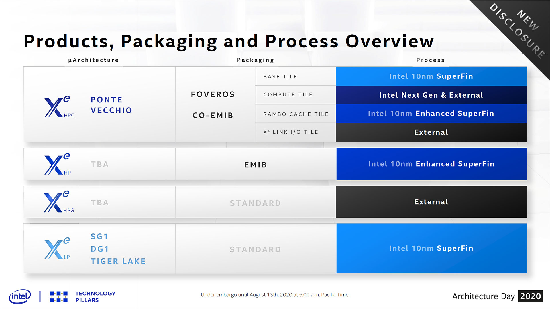
The Xe HP chips won't be going into consumer graphics cards either; that task has been forked over to the Intel Xe HPG, a GPU targeted at enthusiast gamers that will cut out the HPC (high performance computing) elements and add in ray tracing hardware. Xe HP will use Intel's 10nm SuperFin process, however (actually the next step 10nm Enhanced SuperFin), which is the new name for the "10nm++" node that's being used for the upcoming Tiger Lake CPUs.
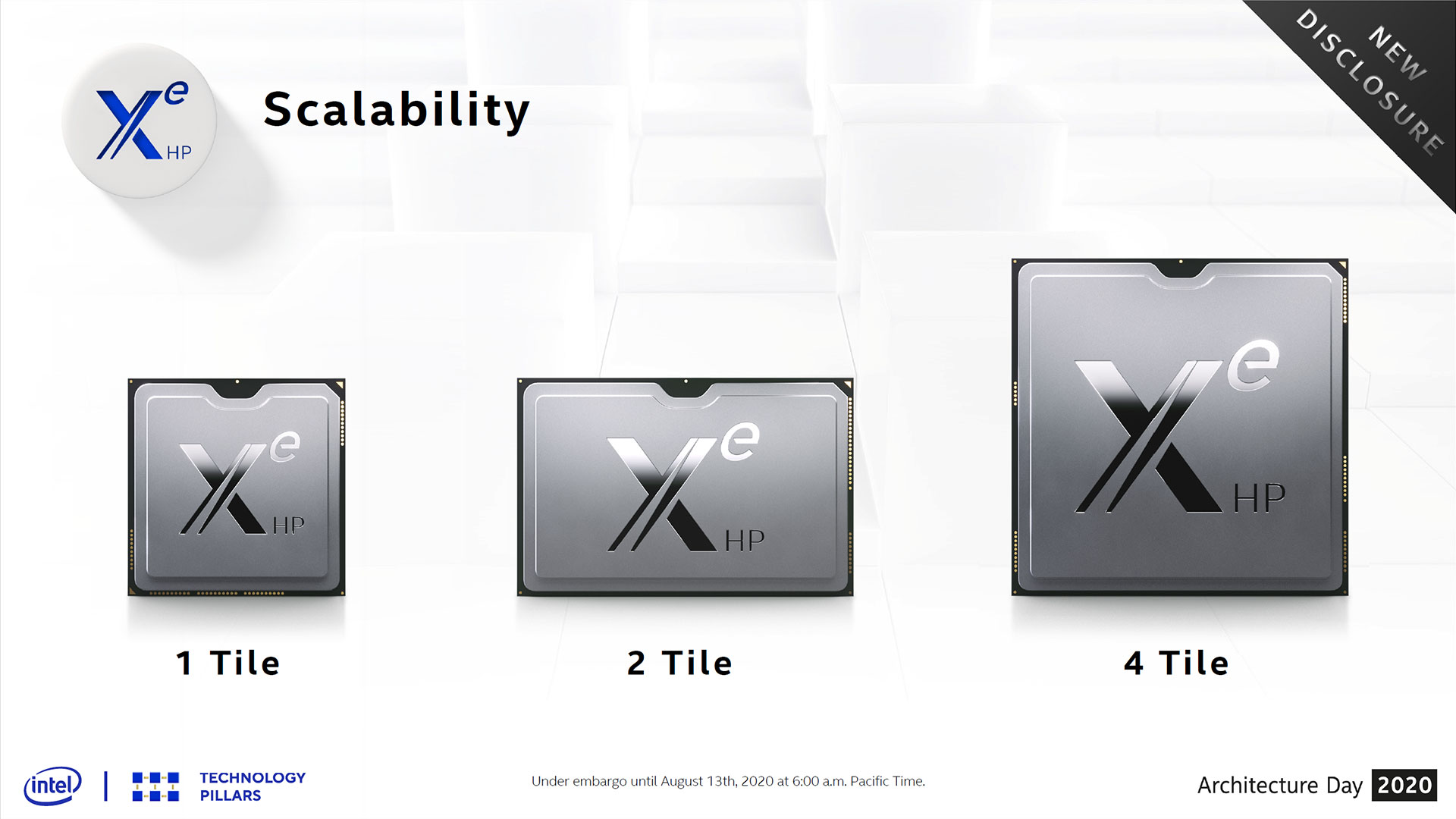
The Xe graphics architecture (you can read more about it in our Xe LP Graphics overview) was designed to scale from teraflops (i.e., consumer level hardware) all the way to petaflops (i.e. supercomputers), with Intel Xe HP / HPC going after the latter. The base design consists of a single tile, Intel's name for a monolithic GPU focused on vector and matrix compute. We'll get into the specs in a moment, but the important thing is that via EMIB (Embedded Multi-die Interconnect Bridge) for the current generation, and Foveros (die stacking) and Co-EMIB for the future Xe HPC Ponte Vecchio, Intel can scale from a 1-tile implementation up to 4-tile solution. Because of the high-speed interconnects, the 1-tile, 2-tile, and 4-tile solutions all appear as a single GPU instance, just with far more performance in the latter.
Article continues belowWe've seen several images of Xe HP over the past several months, and now we know precisely what each one represents. The single tile solutions is a pretty big chip in its own right, but it's dwarfed by the 2-tile and 4-tile packages. There have been hints that Xe HP is close to the maximum reticle size for a microprocessor (around 850 mm2), and the 2-tile package doubles down on that, and then the 4-tile doubles down again. The full-fat 4-tile package looks to be in the neighborhood of 60x60 mm — maybe even a bit larger.
So what sort of hardware does Intel put inside Xe HP? For starters, each tile appears to have two HBM2e stacks, potentially providing up to 32GB of memory and 820 GBps of bandwidth. We don't have specifics on the clocks or capacities Intel is using for the HBM2e stacks, but at least 16GB total seems likely.
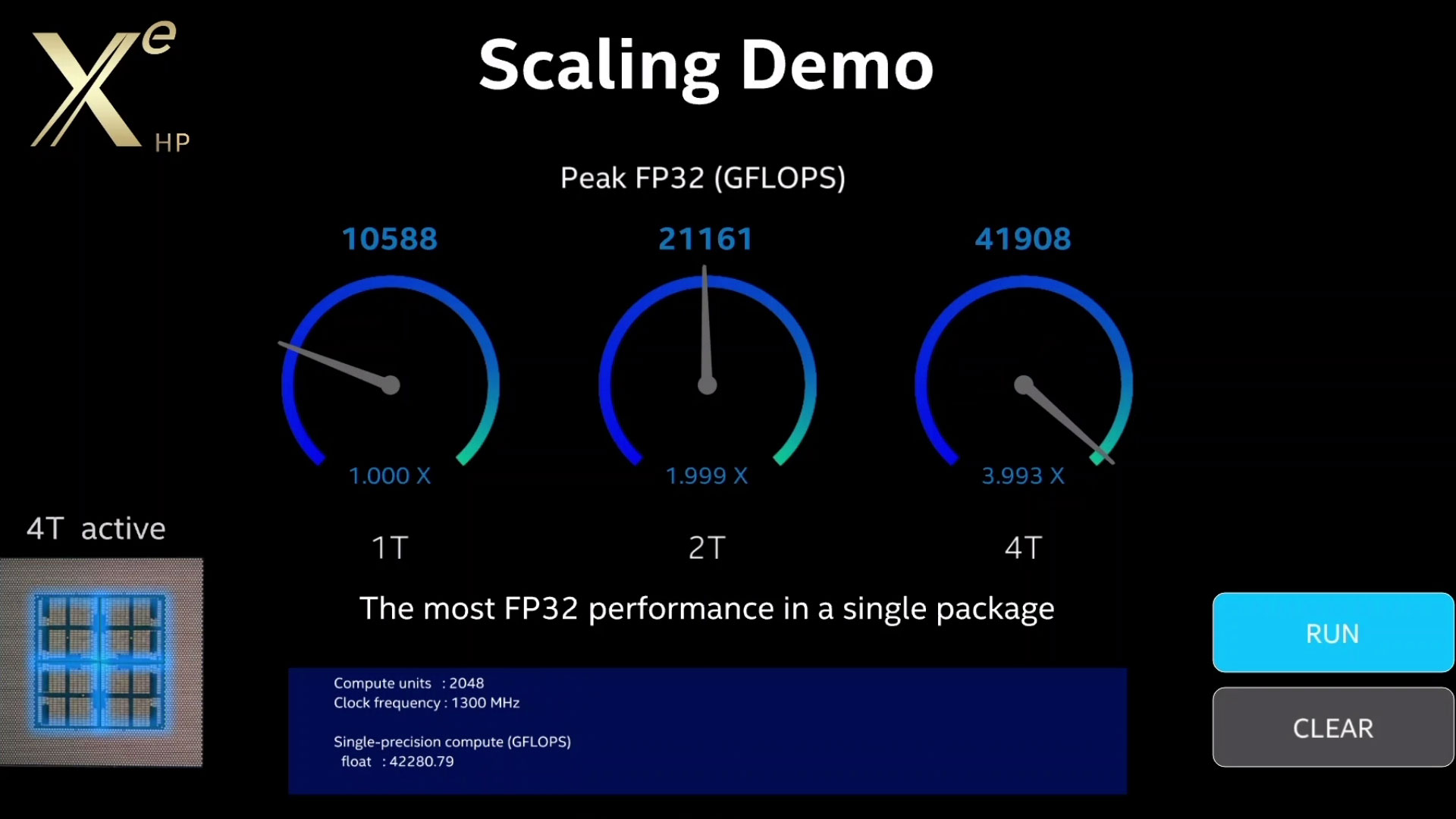
Moving to the GPU itself, Intel provided significantly more details. While it hasn't said whether it's the maximum configuration or not, Intel showed a compute demo running on 1-, 2-, and 4-tile implementations, with each tile sporting 512 EUs. This is what we've expected for a while, but it was nice to have that at least confirmed. This is still early drivers and hardware, but we also saw clock speeds of 1300 MHz.
The math follows pretty easily from there. Each EU has eight FP/INT ALU pipelines, capable of doing a single FMA (fused multiply add) operation per clock:
Get Tom's Hardware's best news and in-depth reviews, straight to your inbox.
8 × 512 × 2 × 1.3 GHz = 10,649.6 GFLOPS
That's for a single tile, so multiply that by two or four for the larger solutions. That's a theoretical 42.6 TFLOPS for the 4-tile configuration, and Intel's demonstration at least suggested that the hardware can get pretty close to that figure: 42,280.79 GFLOPS. Of course we have no way to know whether the software was really running those computations or if it was just a faked animation, but we'll leave it at that for now.
The Xe HP GPU also has the ability to do FP64 operations, presumably at half the performance of FP32. It also supports INT8 for deep learning applications that don't require the precision of FP32. Based on what we know of the Xe architecture and assuming linear scaling, that means up to 42.6 teraops of INT8 for a single tile, or 170.4 TOPS for the 4-tile version.
Not surprisingly, Xe HP doesn't focus solely on standard GPU-type processing clusters. Like Nvidia's V100 and A100 (and Google's TPUs, Tensor Processing Units), Xe HP also includes tensor-style capabilities that should further improve computational performance. Like the A100 and TPU3, Xe HP also supports the bfloat16 format, which offers similar accuracy for AI purposes to FP32 but at twice the performance. (Technically, it has a wide range of values thanks to the 8-bit exponent, but limited precision of only 7-bits.)
Xe HP isn't ready to ship quite yet, and Intel didn't go into deeper details on the tensor computational performance, but it's reasonable to expect even more performance potential than the standard FP ALUs can provide. Whether it will be enough to match Nvidia's A100 remains to be seen, but Intel has exascale ambitions. Given what was revealed today, all Intel needs to do is put together a supercomputing cluster with about 25,000 Xe HP 4-tile nodes and it could get there. And if the tensor processing is eight times as fast as the standard ALUs, maybe Intel can make do with only 3,000 Xe HP nodes in the cluster. Simple!
The exascale ambitions don't fall under the Xe HP nomenclature, however. Instead, they're classified as Xe HPC, also codenamed Ponte Vecchio. Previously, Ponte Vecchio was supposed to be Intel's first 7nm part, but now Intel says it will be manufactured using 10nm SuperFin for the base tile, with 10nm Enhanced SuperFin for the Rambo Cache tile. So far so good, but then we get some fuzziness. The compute tile will use "Intel next gen," which presumably means 7nm, or "external" — meaning Samsung or TSMC 7nm most likely. The Xe Link I/O tile is also listed as using external manufacturing.
Intel has already demonstrated the ability to use Foveros stacking with externally manufactured silicon, so this can all still come together in time for the 2021 launch of the Aurora supercomputer. Whether it's via 10nm SuperFin or 7nm or some other process, Intel hasn't stepped back from its exascale ambitions.

Jarred Walton is a senior editor at Tom's Hardware focusing on everything GPU. He has been working as a tech journalist since 2004, writing for AnandTech, Maximum PC, and PC Gamer. From the first S3 Virge '3D decelerators' to today's GPUs, Jarred keeps up with all the latest graphics trends and is the one to ask about game performance.
-
setx ReplyXe HP also supports the bfloat16 format, which offers similar accuracy to FP32 but at twice the performance
Please read something before you write such nonsense.
BFloat16 has the same range as FP32 but precision(accuracy) is much worse. -
JarredWaltonGPU Reply
I've clarified that this 'accuracy' is specifically for machine learning purposes.setx said:Please read something before you write such nonsense.
BFloat16 has the same range as FP32 but precision(accuracy) is much worse. -
Deicidium369 WCC had an exclusive stating that initially a 6nm TSMC process would be used, which is a slightly more dense 7nm - the updated exclusive is that will be on TSMC 5nm - as it is roughly the same density as Intel 7nm - this will NOT be a super high volume part - likely this arrangement just for the Aurora Exascale - which was 1st 7nm to have "shipped" - and the one put back 6-12 months.Reply
Rocket Lake - Late 2020 - 14nm
Alder Lake - Late 2021 - 10nm
Meteor Lake - Late 2022 / Early 2023. - 7nm
~1 year cadence
Ice Lake SP - Late 2020 (very short platform life) 10nm
Sapphire Rapids - Mid to Late 2021 - 10nm
(will be a long platform, unlike Cooper Lake / Ice Lake SP)
Granite Rapids - 2022/ 2023 - 7nm
Sapphire Rapids reunified the Xeon for 1-8CPU - and will likely be a longer term platform - with Granite Rapids being just a shrink - later in the platforms life.
So looks like the PVC was the part pushed back 6-12 months - Not like we were going to get Rocket Lake and 6 months later Alder and 6 months after that Meteor
https://wccftech.com/exclusive-intel-ponte-vecchio-gpu-not-on-tsmc-6nm/


