Rambus Making Mobile Memory More Efficient
Good news for your battery in your device from the future.
Get Tom's Hardware's best news and in-depth reviews, straight to your inbox.
You are now subscribed
Your newsletter sign-up was successful
Earlier this year, we brought you details of Rambus' "Mobile Memory Initiative" (MMI), which focuses both on high speed and low power memory technologies. Rambus says that it is targeting data rates of 4.3 Gbps, which could facilitate more than 17 GB of memory bandwidth from a single DRAM.
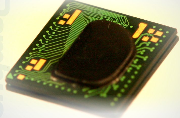
Today Rambus announced that it has evolved the technology further in its second generation silicon, which brings its high-bandwidth mobile memory controller to an achievable power efficiency of 2.2mW/Gbps.
This is nearly a one third improvement over the initial MMI silicon that ran at 2.3mW/Gbps – a fact that Rambus boasts that is significantly better than the estimated 10mW/Gbps of an LPDDR2 400 memory controller. Rambus told us that the gain in power efficiency was achieved through design and not a process shrink.
“The performance demands of next-generation mobile devices are vastly outstripping the pace of battery technology improvements,” said Martin Scott, senior vice president of Research and Technology Development at Rambus. “With the innovations developed through our Mobile Memory Initiative, we can deliver advanced applications and maintain long battery life through our breakthroughs in both bandwidth performance and power efficiency.”
To recap the three technologies Rambus pushes for its MMI:
The first is Very Low-Swing Differential Signaling (VLSD), which aims to keep performance up while minimizing power consumption.
The second is what Rambus calls a “FlexClocking Architecture,” which utilizes asymmetric partitioning and places critical calibration and timing circuitry in the controller interface, greatly simplifying the design of the DRAM interface and also reducing power needs.
Get Tom's Hardware's best news and in-depth reviews, straight to your inbox.
The third technology is an advanced power state management system that ensures that the memory is only powered up when needed. The architecture provides quick transition times between three power states, ranging from full power on both the DRAM and memory controller to a deep power down where only leakage power is consumed.
-
darkknight22 awesome. hopefully it won't cost me my firstborn child if i ever want to add more later.Reply -
IronRyan21 It seems Rambus will never die. Nothing can destroy it..........Its immune to lawsuits, competition, outdated technology.........Reply -
ricardok So now Rambus is creating stuff? Nice to see that.Reply
All I can remember from Rambus was them suing every memory maker on the market.
It's good news that they started producing/creating new things instead of new lawsuits. ;) -
This ought to be really interesting! :)Reply
Wonder when they'll start manufacturing PC memory for consumers, what form it'll take and how many Gigs there'll be per stick? -
ta152h Is everyone forgetting how good RDRAM was, when Intel used it properly?Reply
The lawsuits get tiring, for sure, although I can hardly blame them since they make money from them, and get others to sign licensing agreements, but to comment negatively on Rambus' technology is ill-informed. They have come out with some interesting stuff, and useful products, and still do. There was a time when getting a Pentium 4 without RDRAM was accepting a big loss in performance, compared to DDR. Intel created the i850 and never did anything with it, but it was still the fastest chipset for the Pentium 4 for a long time, despite newer ones from competitors and Intel.
Even for the Pentium III, with the very limited FSB, the i840 was the fastest chipset in dual-processor configurations, by a lot. In single processor setups, the overclocked 440BX could beat it in some. RDRAM wasn't a bad technology, it was just Intel used it too soon (prices were astronomical) and for a processor that couldn't hope to use the bandwidth, and it still performed pretty well.
Don't forget, XDR is used in the PS3, the best selling console in September (I never thought I'd be able to say that :-P ).
Rambus is viewed negatively, and some of it is justified, but it's gotten so extreme it's become exaggerated and uninformed. -
NoCaDrummer I wouldn't buy a PC with it, after the skanky way they get other manufacturers to sign on to a "standard" that they just happen to own the patents on. It may be good for their business (money-wise) but it's a lousy way to gain trust. To paraphrase a former First Lady, "Just say 'No' to Rambus!"Reply

