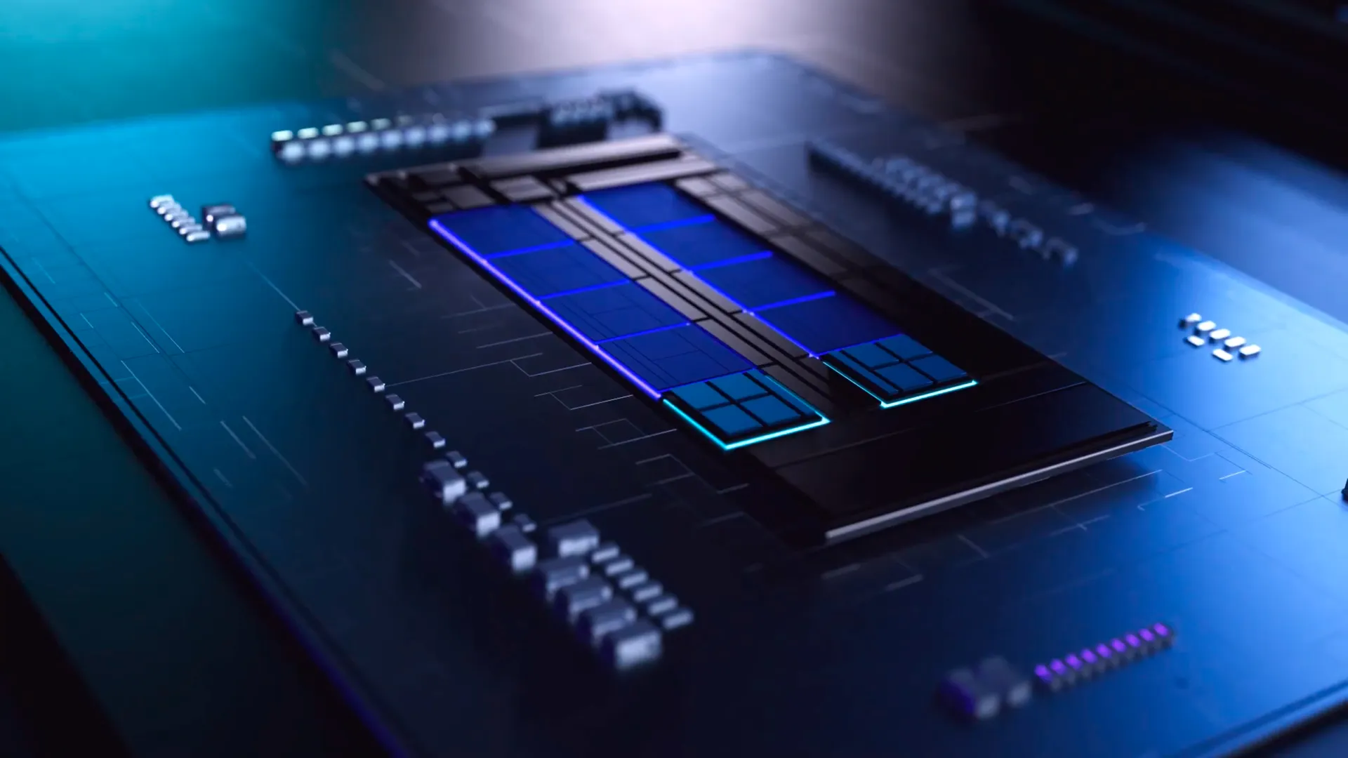
A content creator on the Bilibili video platform has obtained an engineering sample of Intel's Core i9-13900 Raptor Lake processor and delidded the chip on video for everyone to see. As a result, we now know the official dimensions of Intel's Raptor Lake CPU die, measuring 23.8 by 10.8 mm. This translates to a slightly wider and much longer die size compared to 12th generation Alder Lake CPUs.
Near the end of the video, the content creator put three delidded chips together from the past, present, and future generations of Intel CPUs, including the Rocket Lake Core i9-11900K at 24 x 11.7 mm, Alder Lake Core i9-12900K at 20.4 x 10.2 mm, and of course the Raptor Lake i9-13900 engineering sample. The Raptor Lake part sits in-between the two other chips in size, with the i9-12900K being the smallest chip of the bunch, and the 11900K being the largest of them all.
Raptor Lake's die size translates perfectly into the architecture's new enhancements we've been hearing about for months. These changes include doubling the core count of the efficiency cores, a massive bump in L2 cache—by 60%—and a small bump in L3 cache as well.

These additions are undoubtedly the reason why Raptor Lake's die size has lengthened by a fair amount. The additional core count requires two more quad-core clusters to be fused onto the architecture, which requires a lengthier die to fit onto the chip without shrinking any of the other components.
We can't be sure why the die size has widened as well, but we assume it's related to the large L2 cache sizes, which might need some more room to fit onto the entire package. There is also a chance the new but unofficially confirmed "Raptor Cove" performance cores are affecting the die size as well. But, since we have no concrete data on any changes Raptor Cove has over Golden Cove (Alder Lake's P cores), we cannot be certain.
One thing worth mentioning is the die size of Intel's previous generation Rocket Lake i9-11900K, versus the i9-13900. With a die size still larger than the Raptor Lake architecture, despite the addition of two more core clusters. This data puts into perspective how genuinely woeful Intel's 11th generation architecture was.
For the uninitiated, Rocket Lake has been regarded as one of Intel's worst architectures to date, with some calling it a failure altogether. The CPU architecture was a step backward in many ways compared to its 10th generation Comet Lake predecessor, with the architecture itself being specifically designed for Intel's latest (at the time) 10 nm process. But thanks to development issues, the 10 nm node had to be delayed, forcing Intel to backport Rocket Lake to its larger 14nm process.
As a result of the node change, Rocket Lake's die size grew tremendously, while core counts were reduced at the exact same time, going from 10 to 8 on the flagship i9 models. Even worse, Rocket Lake also consumed more power than its predecessor with peak power hitting around 300W for the flagship part in our power results.
Thankfully the architecture still had its IPC improvements intact and featured the AVX-512 instruction for the first time ever on a mainstream platform. So the architecture wasn't a complete flop. However, its ridiculous power requirements, combined with reduced core counts put a sour taste in many people's mouths.
Back to Raptor Lake - Intel's new 13th gen chips will be compatible with the current LGA 1700 socket despite the large die, and will be compatible with LGA 1700 coolers and current 600 series chipset motherboards from Intel - with the only requirement being a simple BIOS update.
The large die size could put more work into the CPU coolers, with additional heat generated by the cache and cores, but we don't expect it to be a significant change over Alder Lake. These chips will need to reside under a similar power envelope as their Alder Lake predecessors either way.
Raptor Lake still does not have an official release window, but all rumors point to a Q4 2022 launch right now, which aligns well with AMD's confirmed Ryzen 7000 series launch in Q4 as well.