Samsung Preps Next-Gen V-NAND Memory: Higher Capacity and Performance
Samsung's 200-layer V8-NAND is getting closer.

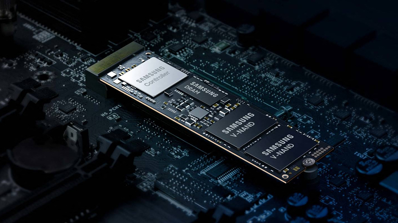
Samsung is getting ready to start mass production of its 8th Generation V-NAND memory, which will feature over 200 layers and bring higher performance and bit densities for solid-state storage devices.
Samsung was years ahead of its competitors with its 24-layer V-NAND flash memory in 2013, and it took other companies quite some time to catch up. But since then, the South Korean giant has become a bit more cautious as it has become harder to build NAND with hundreds of layers. This year Micron and SK Hynix beat Samsung to punch with their 232-layer and 238-layer 3D TLC NAND devices. But the V-NAND developer is not standing still and is getting ready to start volume production of 3D NAND memory (which will be branded V-NAND, of course) with 236 layers, reports Business Korea.
Samsung produced the first samples of its V-NAND memory with over 200-layers in mid-2021, so it should now have enough technology experience to initiate volume production of such devices. Unfortunately, at this point, it is hard to tell the capacity of Samsung's upcoming 8th Generation V-NAND chips. Still, we are sure that one of the company's goals with its next-generation NAND memory will be faster interface speeds and other performance characteristics to enable next-generation best SSDs.
To build competitive solid-state storage solutions for upcoming desktops and laptops with a PCIe Gen5 interface and smartphones supporting UFS 3.1 and 4.0 interfaces, Samsung needs NAND devices with a high-speed interface. Today's Samsung's V7-NAND already features interface speeds of up to 2.0 GT/s, but we expect the company to increase interface speed with its V8-NAND further.
Another thing to expect from Samsung's 8th Generation V-NAND is increased program block size and decreased read latency, which optimizes the performance of high-capacity 3D NAND devices. But unfortunately, the exact characteristics are unknown.
While an increased number of NAND layers is sometimes considered an easy way of flash memory scaling, it is not. Making NAND layers thinner (and therefore NAND cells small) entails using new materials to store charges reliably. Furthermore, since it is challenging (and maybe not feasible economically) to etch hundreds of layers, 3D NAND makers need to adopt techniques like string stacking to build 3D NAND with hundreds of layers. Samsung has not yet adopted string stacking with its 176-layer V7-NAND, but it remains to be seen whether the technology will be used for 236-layer V8-NAND.
Get Tom's Hardware's best news and in-depth reviews, straight to your inbox.

Anton Shilov is a contributing writer at Tom’s Hardware. Over the past couple of decades, he has covered everything from CPUs and GPUs to supercomputers and from modern process technologies and latest fab tools to high-tech industry trends.
-
hotaru251 is it wise to invest so far in future v-nand where u dont even use the older generation yet?Reply
As the recent X-nand seems to be best option going forward (due to SLC speed w/ qlc capacity) right? -
Alvar "Miles" Udell ReplyStill, we are sure that one of the company's goals with its next-generation NAND memory will be faster interface speeds and other performance characteristics to enable next-generation best SSDs.
Probably, they want the speed numbers only 0.01% of people will see (as it requires data center level queue depths), they don't care about capacity that 100% of people need.