Semiconductor Researchers Solve Diamond Wafer Slicing Challenges With Lasers
The laser-based technique may unlock the promise of diamonds as a practical semiconductor material.

Despite all its winning qualities for semiconductor industry use, diamond has been held back as it has been hard to fashion into usable wafers. On Tuesday, a representative from Chiba University in Japan emailed us about a breakthrough described as a novel laser-slicing technique for diamond semiconductors.

Apparently, the scientists have developed a laser-powered process for "effortlessly slicing diamonds." It is thought that semiconductors created using this material will be prized for their use in highly efficient power conversion components in electric vehicles and for high-speed communication technology.
Diamonds can be very particular in how they are sliced due to the inherent crystallographic planes. These planes don't conform to a semiconductor maker's desires for producing grids of wafers. Thus, creating and slicing diamond wafers has been difficult, and often wasteful — and they aren't cheap.
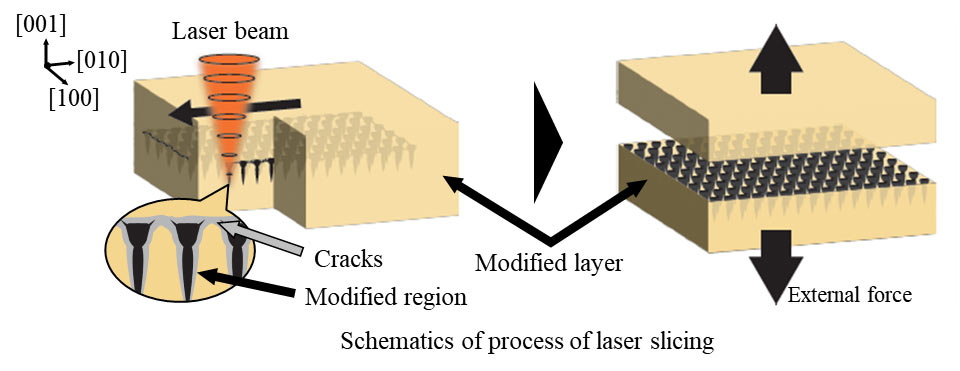
So, how does a laser help in the manufacturing of diamond wafers? The research team describes a process where the laser doesn't cut the diamond into a grid, but the "concentrated laser illumination transforms diamond into amorphous carbon, whose density is lower than that of diamond." The resulting lower-density grid line in the diamond structure provides pre-defined fracture planes for cracks to propagate along.
Once the diamond has been treated as described above, the researchers indicate it was easy to separate regular-shaped diamond wafers ready for fabrication work further down the line.
Professor Hirofumi Hidai, from the Graduate School of Engineering at Chiba University, said that "diamond slicing enables the production of high-quality wafers at low cost and is indispensable to fabricate diamond semiconductor devices."
The professor also mentioned the potential of diamond semiconductors in high-power applications like electric vehicles. We have previously reported on the appealing qualities of diamond transistors — many of which stem from the material's natural wide bandgap semiconductor properties. Meanwhile, there are other reports that suggest diamonds might enhance the audiophile qualities of your Ethernet cables…
Get Tom's Hardware's best news and in-depth reviews, straight to your inbox.
Researchers have been on the lookout for promising new semiconductor materials in recent years, as silicon starts to approach its limits, and this new development marks yet another tentative step in a new direction.

Mark Tyson is a news editor at Tom's Hardware. He enjoys covering the full breadth of PC tech; from business and semiconductor design to products approaching the edge of reason.
-
LostFate Great... Now I have to replace all my gold plated, zero oxygen, fiber optic cables again...Reply -
Eximo Freakin' laser beams.Reply
Basically they are saying that adding a lot of energy turns it from diamond to some other carbon allotrope and then they just break it, or it breaks, upon the lines made by the laser.
Not sure why this wasn't a thing before?
Deliberately reaching out to news outlets is not a great sign... -
InvalidError Reply
Sub-surface laser focusing is how multi-layer BD discs work and also how designs get etched in acrylic cubes. Not really a new process, just a new higher-energy, higher-precision application for it.Eximo said:Not sure why this wasn't a thing before?
Great, they solved the diamond-slicing problem. Still got to work on growing cheaper diamond wafers. Not sure the consumer electronics and automotive space is sufficiently concerned about efficiency to spend $60 000 per 3" diamond wafer just to gain another 1-2% on efficiency.

