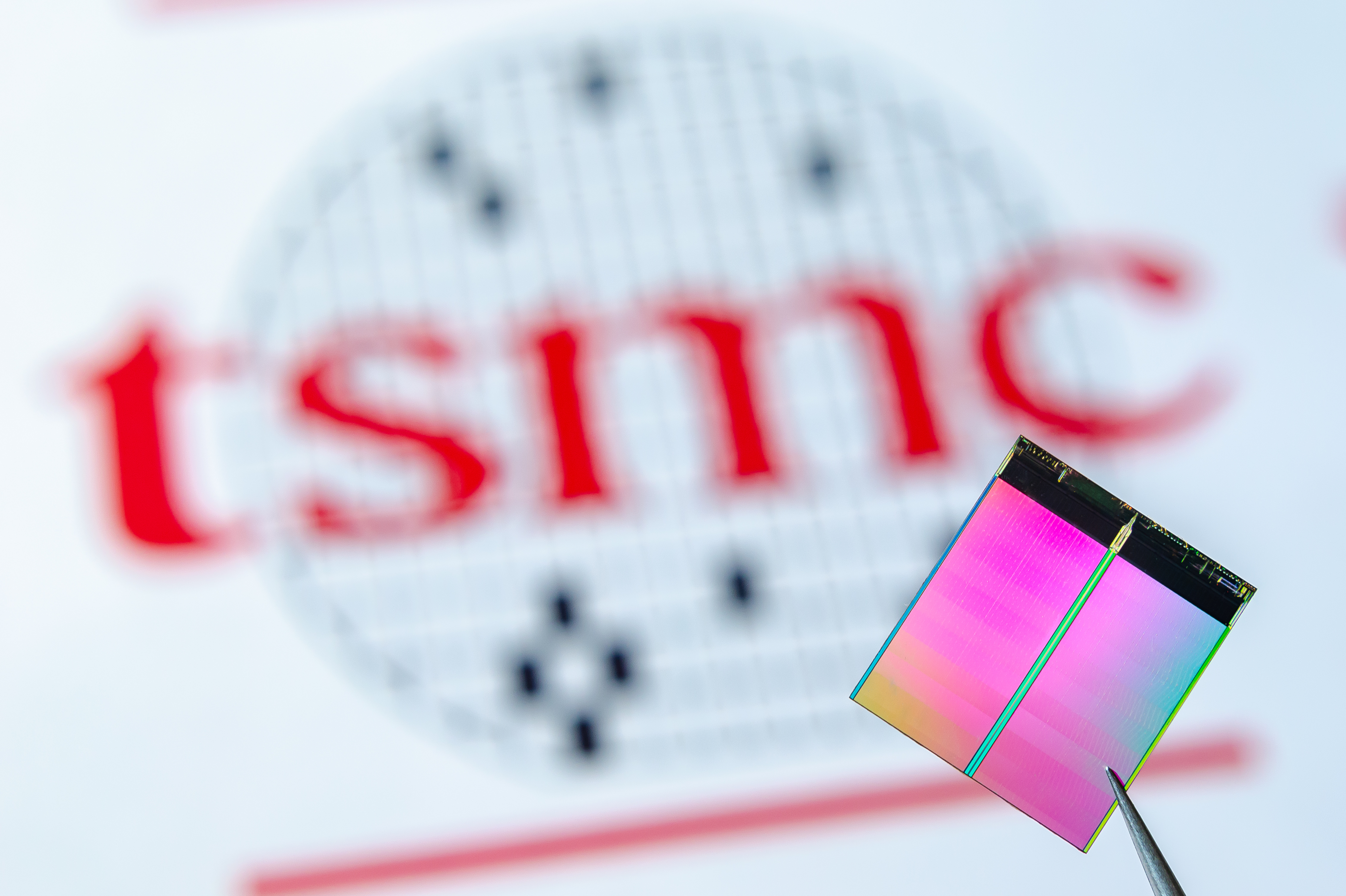
TSMC Starts $19.5 Billion 3nm Fab Construction
TSMC plows forward with 3nm plans
TSMC reportedly has started construction of its 3nm fab that is expected to begin production in 2023. The Taiwan-based contract chipmaker has acquired 30 hectares of land for the facility.

The land is located in the Southern Taiwan Science and Technology Park,where TSMC already employs over 10,000 people, but there aren’t many other details. The location is in line with TSMC's disclosure in 2017 and is the same area set aside for 5nm production. During the fab’s initial announcement in 2016, it was reported that TSMC would need 50 to 80 hectares of land and would launch in 2022.
With the news last year that TMSC had been cleared to begin production, the cost was estimated at $19.5 billion and production slated to start in late 2022 or early 2023. Earlier this year, C.C. Wei, CEO of TSMC, said that 3nm development was “going well” and that it was engaging with early customers on the technology definition.
TSMC is currently working on getting its 5nm process node into volume production in the first half of 2020. In early 2018, TSMC broke ground on its Fab 18 for 5nm production. Fab 18 has a size of 42 hectares, 160,000 square meters of cleanroom area, and will have a capacity of over one million wafers per month when all three phases are completed in 2021, providing work for 4,000 people.
The reported 2023 schedule for 3nm volume production would be noteworthy as TSMC has opted for at most a two-year cadence for all of its nodes since 20nm in late 2014. In general, TSMC has opted for shrinks of at most 2x density scaling with a more steady cadence, while Intel introduced the term hyperscaling at 10nm to describe its ambitious 2.7x scaling on 10nm and 2.5x on 14nm.
On Thursday, Intel said that it aimed to go back to a two-year cadence for at least the next few nodes, with 7nm scheduled for release in the fourth quarter of 2021 with a data center GP-GPU with Foveros 3D packaging. This could indicate that Intel’s 5nm and TSMC’s 3nm nodes will go toe-to-toe in 2023. While no details about either process are known yet, Intel claimed it’s “working to recapture process leadership.”
Samsung plans to begin its own 3nm production in 2021, based on gate-all-around (GAA) technology, although its density will not be as high as TSMC’s 3nm. (For Samsung, 5nm is an optimization of its 7nm node.)
Get Tom's Hardware's best news and in-depth reviews, straight to your inbox.
Earlier this month, TSMC sharply increased its capital expenditures guidance for 2019 by $4 billion to a range of $14-15 billion due to high demand. Intel is also heavily investing in capital with an estimated $16 billion investment in 2019. Intel said on Thursday that it will have increased its production capacity (measured in wafer starts per month) by 25% in 2019 and plans another 25% increase in 2020.
-
helper800 I am certainly spitballing but from what I know of quantum physics getting a true stable 3nm transistor is impossible with conventional silicon. Is anyone knowledgable enough to explain this to me and others?Reply
*Edit: I found some information:
“In a finFET technology, the width of the device is quantized. You can have one fin, two fins, three fins or whatever. In nanosheets, you have a fixed number of nanosheets on top of each other. But you can play with the width. Now, you have access to a continuum of device widths, which you didn’t have for the finFET,” Mocuta said. “For example, you want to have an area that drives a lot of current. That could be a buffer. Then, you want to have an SRAM with a very small footprint. There are different needs on the chip that can be met.”
Source:https://semiengineering.com/big-trouble-at-3nm/