TSMC Mulls Another Fab for 2nm & Two Fabs for Advanced Packaging
Further capacity expansions are considered at TSMC

TSMC yet has to disclose details about its N2 (2 nm) fabrication process, but apparently the world’s largest contract maker of semiconductors is confident that demand for this node will be so strong that it is already mulling building an extra fab to meet it, according to the company’s chairman. In addition, TSMC reportedly plans to build two fabs for advanced chip packaging.
TSMC’s N2: One Fab Planned, Another Is Considered
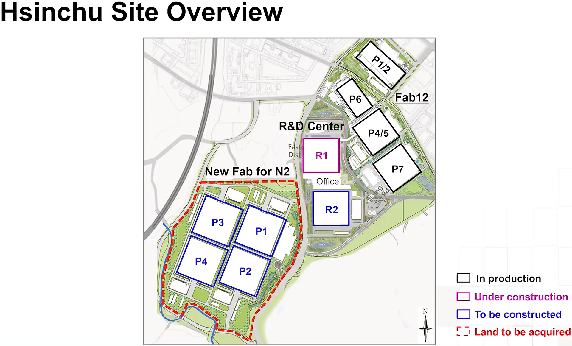
Officially, TSMC’s N2 process is still in in the pathfinding and research mode as the foundry is studying materials as well as viable transistor structures. The home for TSMC’s N2 development as well as initial production will be the company’s site near Baoshan, Hsinchu County, Taiwan, the manufacturer revealed at its Technology Symposium last month. Right now, TSMC is finishing construction of its new R1 R&D facility that will be initially focused on N2 and will start operations next year. TSMC’s first 2nm chips will be made at a new fab that will be built in four phases. At present, the company is in process of acquiring the land for the fab, so there is hardly any solid timeline for the facility that TSMC would like to disclose publicly.
If capacities offered by the new N2 fab near Baoshan are not enough to meet demand, then TSMC will build another leading-edge production facility at its site in Taichung, Taiwan, said Mark Liu, chairman of TSMC, reports DigiTimes.
GAAFETs
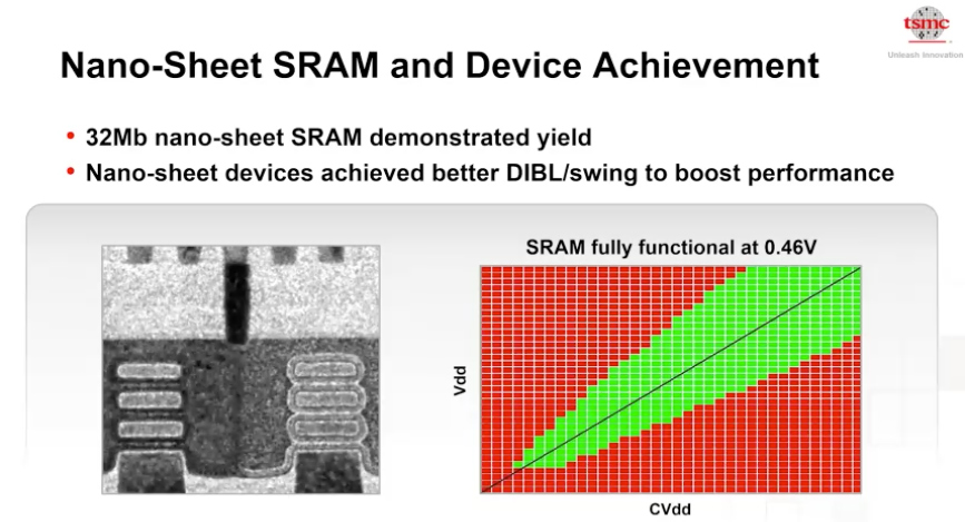
It is generally believed that TSMC will adopt gate-all-around (GAAFET) transistor structure (aka nanowire, nanoribbon, etc.) for its N2 process node. The company has investigated GAAFETs for 15 years and recently demonstrated a working 32Mb nanosheet SRAM prototype at 0.46V, so GAA is the most likely transistor technology for N2.
Switching to a new transistor structure is a big deal not only for TSMC, but also for its partners and clients. The contract maker itself will have to develop all-new libraries with zero re-use of features designed for previous-generation FinFET-based nodes.
Companies like Cadence and Synopsys will have to create an all-new stack of electronic design automation (EDA) tools as well as develop whole new IP libraries. Chip developers will have to adopt completely new design rules and flows as well as remake everything they could have previously re-used from scratch. Last but not least, just like the switch to FinFET structures increased chip design costs back in 2014 – 2015, the adoption of GAAFETs will likely increase design costs once again.
TSMC has not publicly disclosed any schedules for its N2 node. Last month the company revealed that it would start volume production using its FinFET-based N3 process technology in the second half of 2022. Since TSMC usually introduces a new node every year to meet requirements of its large alpha customers, it is logical to expect that in 2023 it will use either a refined version of N3 (e.g., N3+, N3P, etc.), or will start using its N2. In any case, TSMC’s 2 nm technology is at least three years away.
Get Tom's Hardware's best news and in-depth reviews, straight to your inbox.
New Advanced Packaging Facilities Reportedly Planned
Modern leading-edge process technologies are extremely complex and expensive in terms of R&D, production, and chip design. Meanwhile, they do not always provide as significant node-to-node scaling and benefits as they used to a decade or two ago. To that end, in many cases it is not optimal to develop a large monolithic chip made using a leading-edge technology to get a certain level of performance and certain capabilities.
Instead, it makes sense to adopt a chiplet design and produce each chiplet using the most appropriate process. Chiplet integration requires advanced 2.5D packaging and 3D stacking technologies and demand for these technologies is expected to grow rapidly in the recent years.
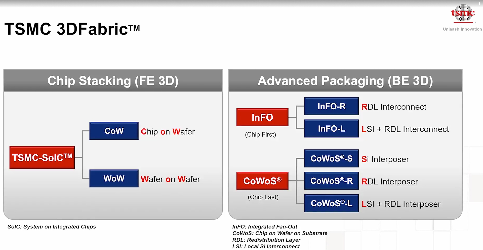
TSMC has a host of advanced 2.5D packaging and 3D silicon stacking technologies collectively known as 3DFabric. TSMC’s logic-on-logic stacking CoW (chip-on-wafer) and WoW (wafer-on-wafer) technologies require advanced frontend production facilities, whereas interposer-based packaging methods like CoWoS (chip-on-wafer-on-substrate) as well as package-on-package interconnects like InFO (integrated fan-out) use backend fab technologies.
While logic-on-logic integration is inherently more complex and expensive than things like CoWoS or InFO, all types of 3DFabric require cleanroom space and such packaging facilities are a far cry from what typical test and packaging factories are. To make the matters somewhat more complicated, advanced processors featuring multiple chiplets are going to use both 3D stacks and 2.5D packages and therefore next-gen packaging facilities have to support both backend and frontend technologies.
At present, TSMC has four advanced packaging facilities in various parts of Taiwan. TSMC projects that demand for its 3DFabric services will be strong in the coming years, so it is prepping to build two more new packaging facilities that will offer both frontend 3D stacking as well as backend CoWoS and InFO packaging processes, reports DigiTimes without disclosing its sources.
One of the fabs will be located in the Chunan section of Hsinchu Science Park, northern Taiwan. The fab reportedly costs a whopping $10.11 billion (according to FocusTaiwan that quoted TSMC’s announcement on Facebook) when fully built and equipped. It will likely be the most expensive test and packaging facility in the industry. It is expected that this fab will come online in the second half of 2021.
Another fab will be located in Southern Taiwan Science Park and is now expected to start volume production some time in 2022.
Sources: DigiTimes (1, 2), FocusTaiwan

Anton Shilov is a contributing writer at Tom’s Hardware. Over the past couple of decades, he has covered everything from CPUs and GPUs to supercomputers and from modern process technologies and latest fab tools to high-tech industry trends.
-
bp_968 Well I hope Intel and Samsung get themselves in gear and competitive. What concerns me about Taiwan is its location and its cultural importance to China.Reply
China could seize the country and strangle a large majority of tech to the world (AMD, Qualcomm, Apple, some Nvidia, etc). Something like that would either cripple most of the world or kickstart WWIII. -
bwohl Very important for the President to entice TSCM to build a couple fabs here in USA...Just in case...Reply -
Kamen Rider Blade Reply
It'll start WW3.bp_968 said:Well I hope Intel and Samsung get themselves in gear and competitive. What concerns me about Taiwan is its location and its cultural importance to China.
China could seize the country and strangle a large majority of tech to the world (AMD, Qualcomm, Apple, some Nvidia, etc). Something like that would either cripple most of the world or kickstart WWIII.
The US has a defense pact with Taiwan.
https://www.anandtech.com/show/15803/tsmc-build-5nm-fab-in-arizona-for-2024bwohl said:Very important for the President to entice TSCM to build a couple fabs here in USA...Just in case... -
thisisaname Reply
They may have a defense pact but they still as far as I can see do not recognize Taiwan as a country.Kamen Rider Blade said:It'll start WW3.
The US has a defense pact with Taiwan.
https://www.anandtech.com/show/15803/tsmc-build-5nm-fab-in-arizona-for-2024 -
DZIrl Yeah 2nm. Marketing crap!Reply
Since 50nm nm means nothing! Just marketing BS. Intel 10nm is in size comparable to TSMC 7nm. Manufacturers use nm and decrease them just to name new process but, as wrote above, has nothing to do with real dimensions.
I'm wondering how will start naming after 1nm.
BTW Si atom is 0.12 nm in size. In this case 2nm means 16 atoms across!! -
DotNetMaster777 Sound very perspective !!! We will see when it is going to happen in Taiwan !!!!Reply
Is it possible to have restriction to sold that in US ???? -
thuckabay World War III is coming, and undoubtedly China and Taiwan will be part and parcel of that: As detailed in the recent book "North Korea, Iran, and the Coming World War: Behold a Red Horse" (see it on Amazon or at Prophecy House's web site ), war is coming, not peace.Reply


