Where Do Hard Drive Heads Come From?
Get Tom's Hardware's best news and in-depth reviews, straight to your inbox.
You are now subscribed
Your newsletter sign-up was successful
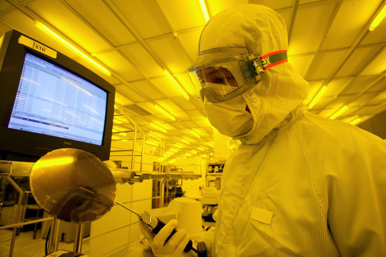
As you might imagine, very few manual operations are performed on the production line. The main role of the operators is to transport the wafers from one stage to another and to oversee proper completion of the operations. To avoid damaging the surface of the wafers, they’re handled by the opposite surface using magnetic spatulas.
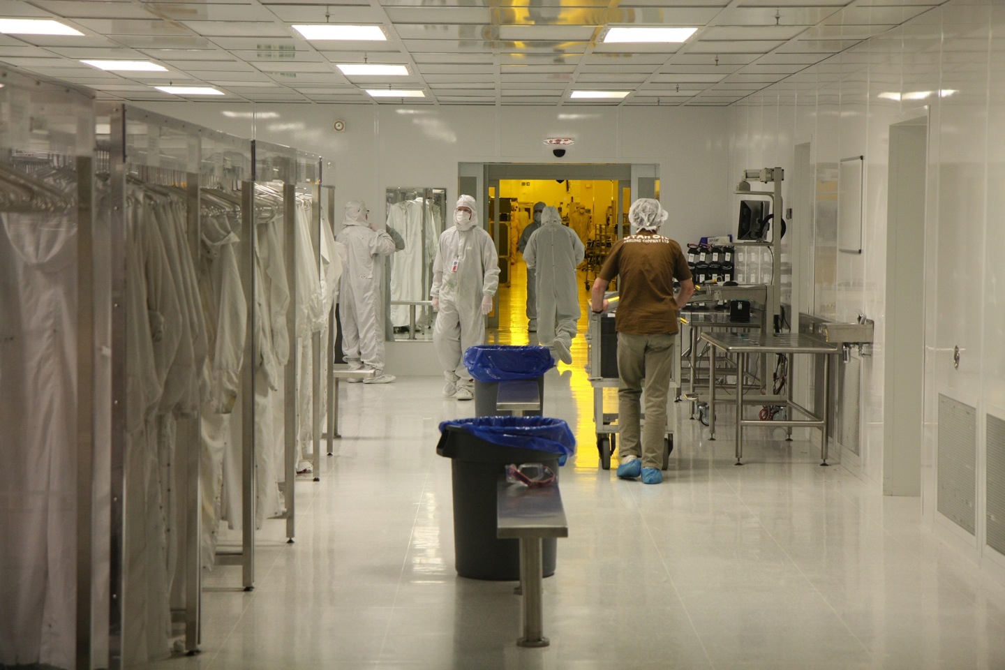
Working conditions are strict. All handling is done in a class 100 clean room, which guarantees no more than 100 particles larger than 0.5 microns per cubic meter of air, and operators must wear protective overalls. Still, the atmosphere is a long way from what you may have seen in the famous Intel ads, with figures wandering around in blue, pink and green hermetic suits.
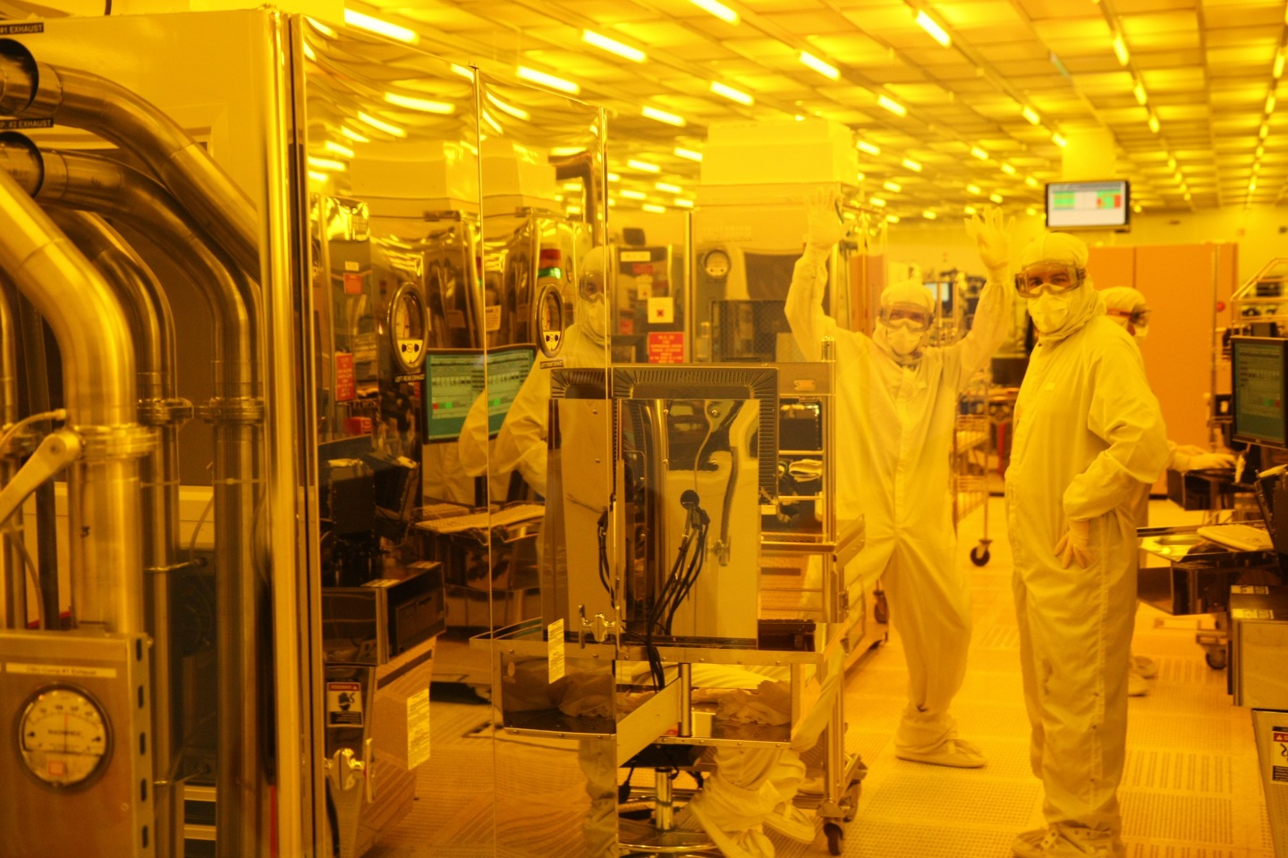
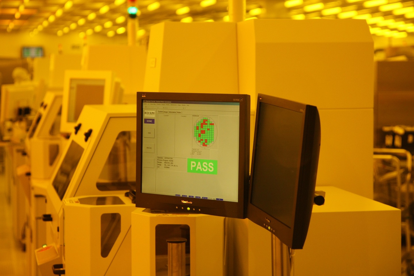
If the yellowish tinge of these pictures has you wondering whether something’s wrong with our camera, don’t worry. The light in the clean room is actually yellow. The reason for this is the same as it is for darkrooms: photolithography requires the surface of the wafer to be sensitive to light, and especially UV light. Using normal white light would ruin the entire surface, so lighting must be highly controlled and limited to precise frequencies that don’t affect the wafers’ light-sensitive coating.
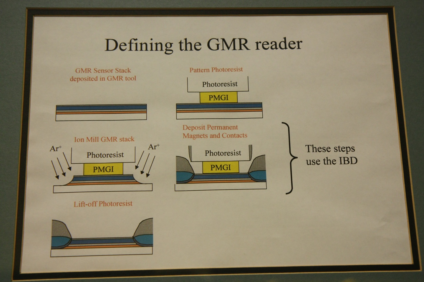
The head fabrication process is so complex that at certain stages it requires removal of part of certain layers that have already been deposited in earlier stages. This is done using selective masking and ion milling. In this process, deposits are cut away by a focused ion beam; once again, all operations are automated. These stages are very time-consuming, since they take place in a high vacuum that takes time to establish (up to two hours) despite the use of large pumps.
The wafers are tested at various stages of the fabrication process. The tests can be optical, via microscope, or electrical, using fine-pointed sensors. As you can see on the screen shown above, the success rate of each stage is not always very high, but Seagate claims yield rates of over 90% of total production. Those figures take into account only the number of valid wafers compared to the total number of wafers used. In fact, it’s possible to resurface a wafer that has failed during fabrication to bring it back to its original state, then send it back to the start of the production line.
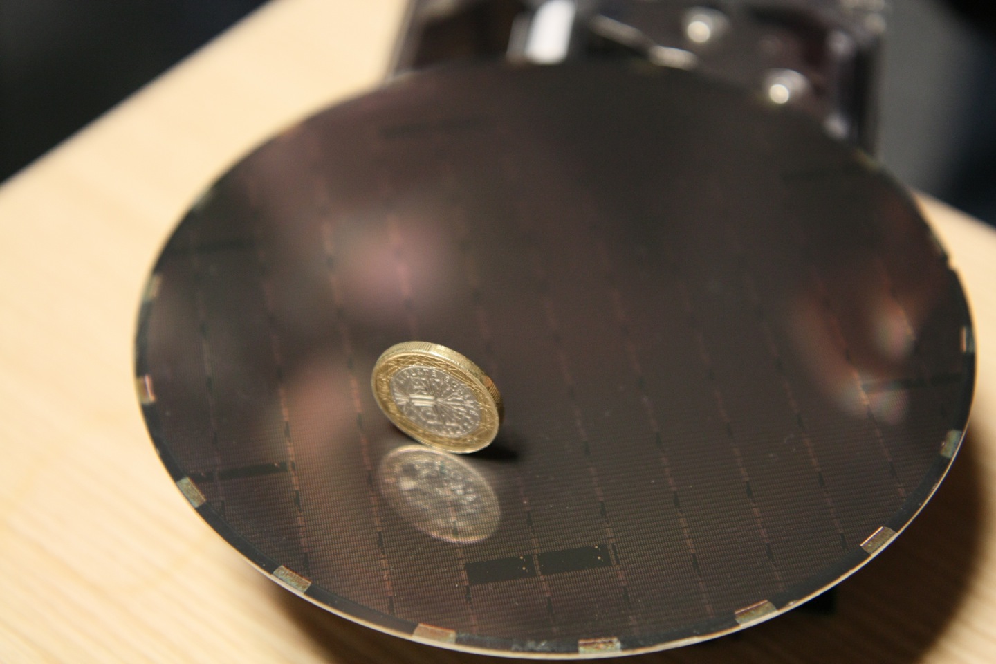
Here’s what a finished wafer looks like. You can easily make out the rows of individual identical heads with the naked eye. The surface of the wafer is perfectly smooth and flat: a real mirror. The heads will later be cut up into strips, which will be cut into individual heads to be mounted onto drive arms.
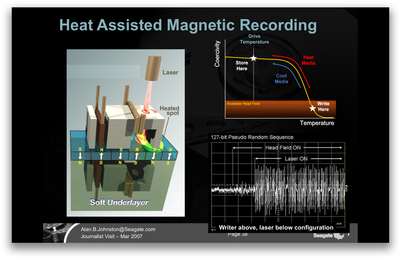
Our tour also gave us the opportunity to talk to Alan Johnston, director of R&D at the Springtown fab, on the changes in hard disk technology we should expect in the coming years. We also touched on how Seagate plans to manufacture 10 TB or 20 TB hard disks, but that’s another topic. It’s worth spending some time on, of course, so we’ll be devoting a special article to it soon. Stay tuned.
In the meantime, you can get more details of our tour by looking at our photo album.
Get Tom's Hardware's best news and in-depth reviews, straight to your inbox.
-
neiroatopelcc "It’s in charge of production of 80% of the magnetic heads used in Seagate hard disks. Springtown has a sister plant in Minneapolis, Minnesota, that provides the remaining 20%." coupled with "Springtown, home to the plant where over 30% of the world’s hard disk read/write heads come from."Reply
Thereby I must conclude that at least 37,5% of the worlds harddrives have seagate read heads ? if that's true, how come hitachi and western digital drives don't fail like their seagate brothers, if it's the same read heads? -
western digital produce their own heads and so do Hitachi. So it's not the same heads. The other brands use TDKs. Plus, I really wouldn't say that Seagate drives are more prone to failure, but I guess you had a bad experience...Reply
-
neiroatopelcc ye I know somewhere it said the rest of the bunch use tdk heads - but that just means that seagate drives must be so common that they are in more than a third of every computer worldwide. Which is unlikely really, since they're hardly the choice for datastores, and aren't really the obvious choice for end users either.Reply
Anyway, ye I have bad experiences with them, but not limited to one drive. What is the worst part of seagate imo isn't the fact that they're failing more than wds - it's that they don't have anything resembling support. You can contact htem, but they'll just say 'that's normal behavour' until the drive fails completely. Then it's your fault it failed. -
Well thats easy to work outReply
Delorean Made in ? questionable build quality?
20% made in USA = 80% left -
I hate WD drives! Not only have I had a bad experience with several WD Drives I had a very bad experience with WD when I tried to get them to make good on one of them. One of them failed under warranty which they replaced only to find out later that they replaced it with an other drive that failed and that they repaired. This drive all so failed and when I called them one of there managers there in word or less told me that I used up my quota and would not make repairs even though it was still under their warranty. This guy told me basically to get lost stating how long did I expect a drive to last. Well my reply was at the least through the warranty period. Even though this happened a while ago I don’t buy WD’s any more and I just cant recommend them. I have used Seagate drives and have had no trouble with them. Since I never had a problem with seagate I cant comment on there customer service. Stay away from Western digital I got burnt bad.Reply
-
fadirocks t1cvrtI hate WD drives! Not only have I had a bad experience with several WD Drives I had a very ...etcUmm so far I had so many HDs from all manufacturers, 2 hitachi, 3 maxtor, 3 seagate, 5 WD, 2 FujitsuReply
out of all only 1 WD totally died because my friend tripped on the wires and let the bird fly!! and Fujitsu had horrible unrecoverable sectors but then that was after 5 years of abuse
Out of my clients: #1 cause of HD failure is User like moving laptop around while hibernating/shutting down the system, dropping the laptop while working and using unprotected or limited protected power source! -
szore I had a problem with several WD HD's. I had RAID array, several drives and I dropped my computer while it was running. WD replaced all of them by UPS within the week. They even up graded an old 36 gig 10,000 RPM raptor to the 76 gig model for nothing. While I am not crazy about WD, I have had a few problems with them in other situations, they did replace 4 drives for me within the week.Reply -
neiroatopelcc t1cvrtI hate WD drives! Not only have I had a bad experience with several WD Drives I had a very bad experience with WD when I tried to get them to make good on one of them. One of them failed under warranty which they replaced only to find out later that they replaced it with an other drive that failed and that they repaired. This drive all so failed and when I called them one of there managers there in word or less told me that I used up my quota and would not make repairs even though it was still under their warranty. This guy told me basically to get lost stating how long did I expect a drive to last. Well my reply was at the least through the warranty period. Even though this happened a while ago I don’t buy WD’s any more and I just cant recommend them. I have used Seagate drives and have had no trouble with them. Since I never had a problem with seagate I cant comment on there customer service. Stay away from Western digital I got burnt bad.When you get a drive from wd it'll be a repaired drive yes. But that's within their right. And so far I've never seen a repaired drive fail.Reply
Anyway, do you have a transcript of the warrenty issue you describe? I would like to see it before I believe it.
fadirocksUmm so far I had so many HDs from all manufacturers, 2 hitachi, 3 maxtor, 3 seagate, 5 WD, 2 Fujitsuout of all only 1 WD totally died because my friend tripped on the wires and let the bird fly!! and Fujitsu had horrible unrecoverable sectors but then that was after 5 years of abuseOut of my clients: #1 cause of HD failure is User like moving laptop around while hibernating/shutting down the system, dropping the laptop while working and using unprotected or limited protected power source!I've had 4 500gb wd drives break, and a raptor drive break - but in the same timespan (4 years) I've seen at least 10 seagate drives break, two of which happened within the last 6 months), and some 25 maxtor drives. Granted most of our work computers have maxtor or hitachi drives .... but still - only 2 hitachi drives failed in the same time 25 maxtor and 10 seagate did...
-
matthieu lamelot neiroatopelccWhich is unlikely really, since they're hardly the choice for datastores, and aren't really the obvious choice for end users either.Reply
You really have a bad opinion about Seagate, don't you ? ;) FYI, they have a 66 % market share in the "enterprise disks" sector, Hitachi and Fujitsu each fighting for half of the rest. And globally, they have a 33 % market share, so, yes, their heads are found in one third of all disks sold every year.
