Incredible High-Resolution Die Imagery Of Nvidia GPUs
Nvidia's "Fermi" GF100 GPU is just over the horizon. With it, comes new technology as well as a new host of cards all vying for your dollar. But before that happens, we take an amazing photographic look into Nvidia's GPUs, present, and past.
Get Tom's Hardware's best news and in-depth reviews, straight to your inbox.
You are now subscribed
Your newsletter sign-up was successful
The Entire Batch!
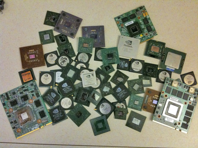
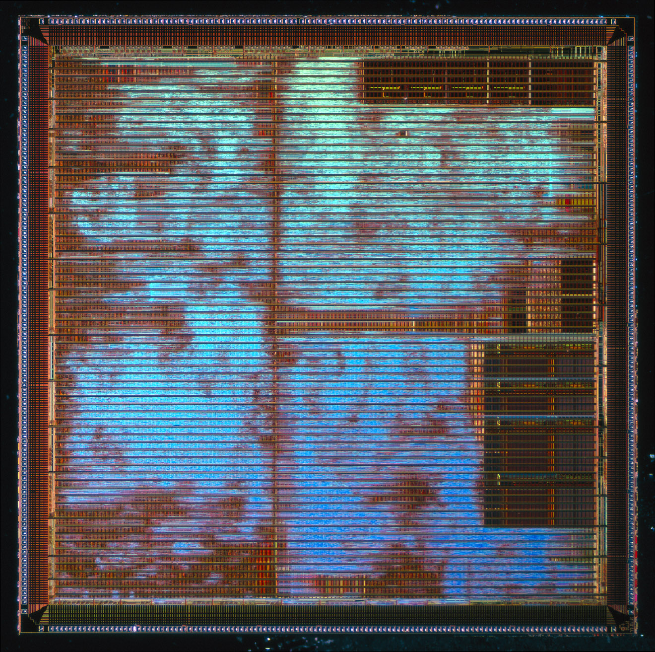
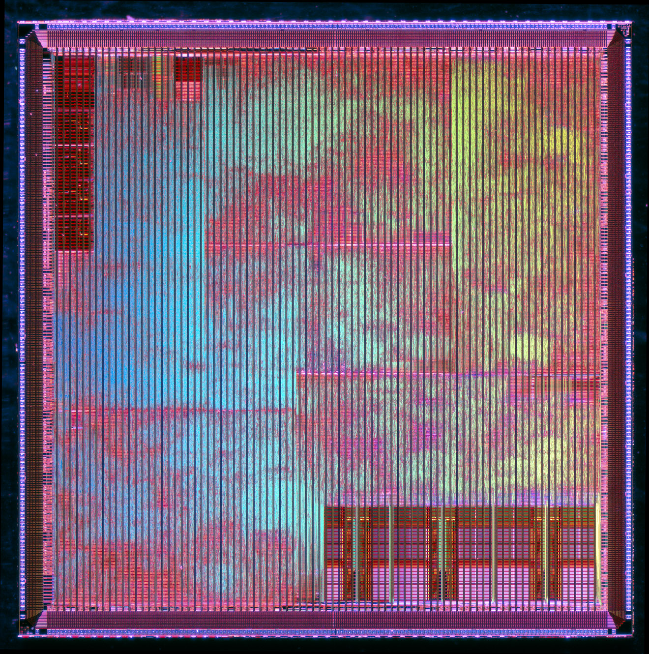
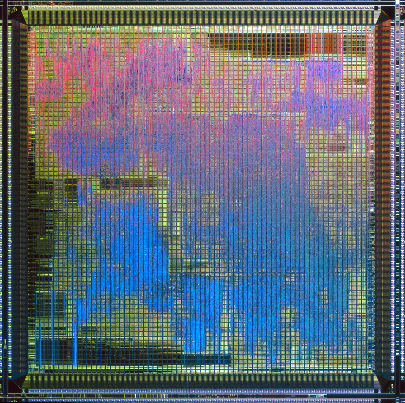
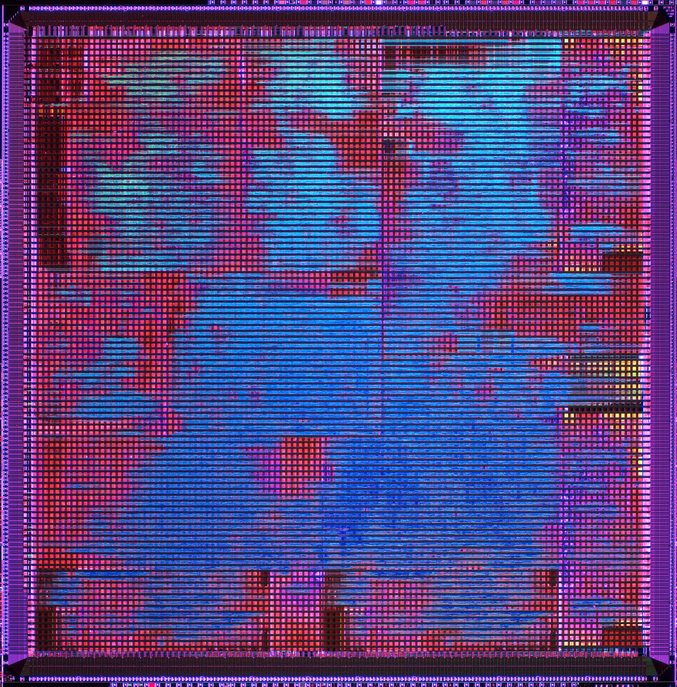
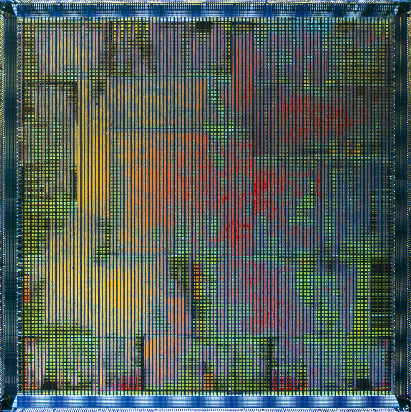
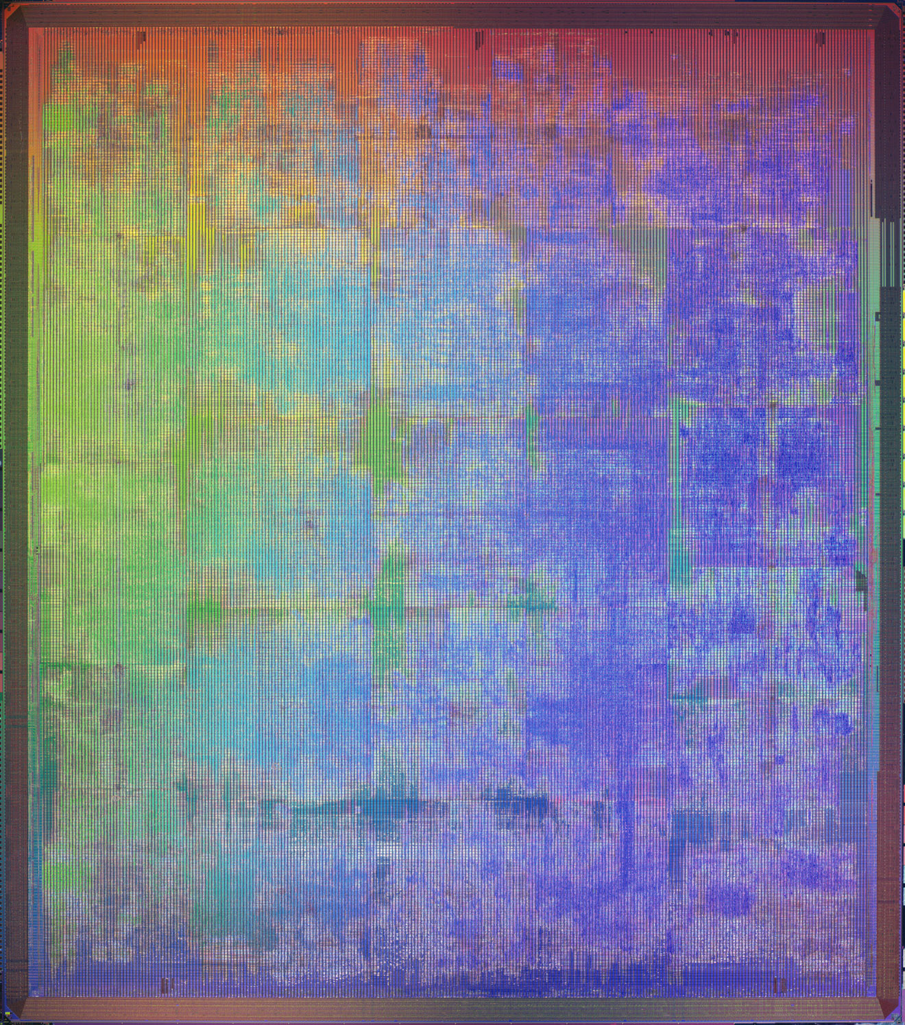
In the above shot, lies essentially every Nvidia graphics chip since NV1--and a few AMD CPUs thrown in for good measure. We were fortunate enough to receive a batch of high-resolution die shots for most of Nvidia's major GPU releases--Thanks Bryan!. We've listed the specs for the core family, and provided the full resolution images for your viewing pleasure.
It's pretty incredible how these things are conceived, designed, and manufactured. Get an inside glimpse of the mind boggling, yet beautiful view of GPU circuitry.
Check out the gallery on the next several pages! Which one was your all time favorite?
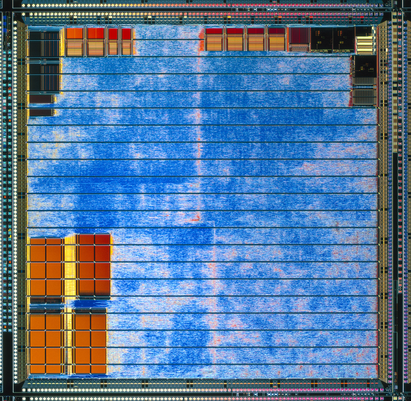
Article continues belowNV4 As The Riva TNT, 1998
NV4.
The TNT really was the start of Nvidia picking up notices in the gaming community. While gamers were torn between 3dfx's Voodoo/2 and TNT, at the time, most still settled on the Voodoo series for the best possible 3D performance.
* 16MB of SDRAM memory
* 90 MHz Core Clock
* 110 MHz Memory Clock
* 180 Megatexel-per-second fill rate
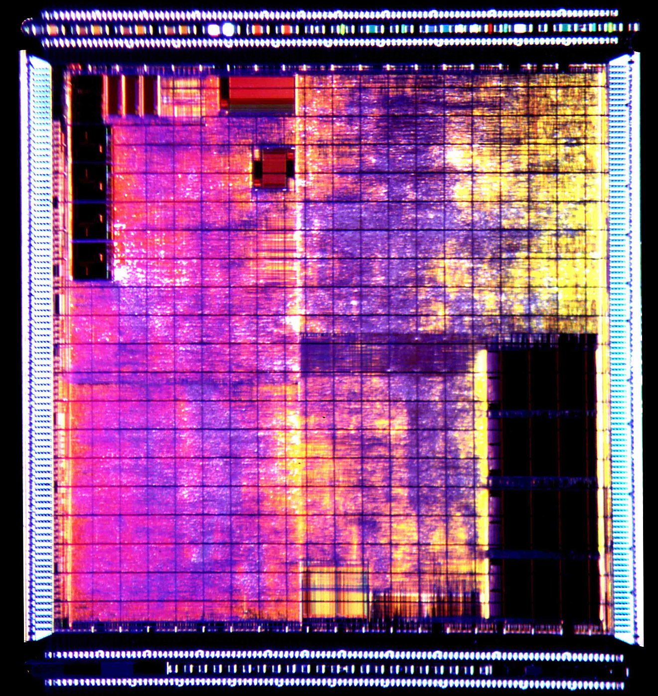
NV5 As The Riva TNT2 Ultra, May 1999
NV5.
Get Tom's Hardware's best news and in-depth reviews, straight to your inbox.
The TNT2 was the first mainstream chip that brought excellent 3D performance that combined both 3D and 2D acceleration together. Previously to this, it was still widely accepted that all in one cards were no match for dedicated 3D cards. The TNT2 (our favorite being the TNT2 Ultra) changed the face of 3D add-in boards forever.
Nvidia's CEO Jen-Hsun Huang told me once that the idea for TNT2 Ultra came from him using a peltier-cooler on the TNT2 chip.
* 32MB of SDRAM memory
* 150 MHz Core Clock
* 183 MHz Memory Clock
* 2.9 GB/s Memory Bandwidth
* 300 million pixels-per-second fill rate
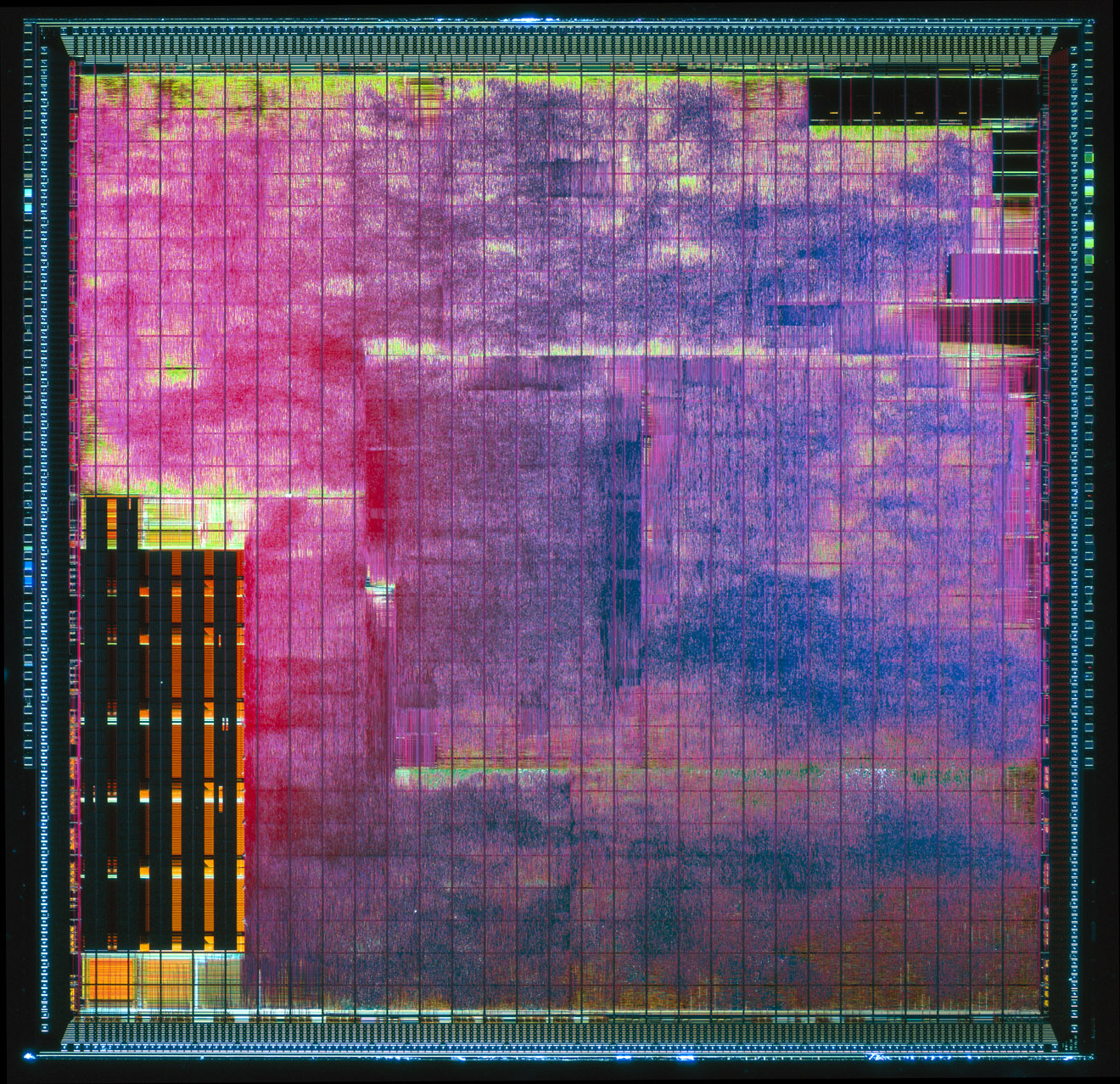
NV10 As The GeForce 256, January 2000
NV10.
Nvidia coined the term GeForce from "geometry" and "Force" to play on the term G-force. And what a force it was. Who can remember the tech demos that Nvidia was releasing at the time? Chameleon anyone?
* 32/64MB of DDR memory
* 120 MHz Core Clock
* 150 MHz Memory Clock
* 4.8 GB/s Memory Bandwidth
* 480 Megatexel-per-second fill rate
NV11 As The GeForce 2 MX, June 2000
NV11.
After much success producing a series of winners in the high-performance 3D category, Nvidia sought out to produce entry-level products to grab even more market share. The GeForce 2 MX was essentially Nvidia saying to the industry "all your base..."
* 32/64MB of SDR memory
* 175 MHz Core Clock
* 166 MHz Memory Clock
* 2.7 GB/s Memory Bandwidth
* 700 Megatexel-per-second fill rate
NV15 As The GeForce 2 GTS, April 2000
NV15.
I never owned one of these specifically, but at the time, the GeForce 2 GTS was a very popular chip. Check out how much memory it came with!
* 32/64MB of DDR memory
* 200 MHz Core Clock
* 333 MHz Memory Clock
* 5.2 GB/s Memory Bandwidth
* 1,600 Megatexel-per-second fill rate
NV17 As The GeForce 4 MX 460, February 2002
The GeForce 4 MX was regulated to entry-level platforms. It also made a large appearance in notebook platforms as well as low profile systems.
* 64MB of DDR memory
* 300 MHz Core Clock
* 550 Hz Memory Clock
* 8.8 GB/s Memory Bandwidth
* 1,200 Megatexel-per-second fill rate
NV20 As The GeForce 3, February 2001
The GeForce 3. By this time, it was widely accepted that "GeForce" would be to Nvidia what "Pentium" was to Intel. The name stuck.
* 64MB of DDR memory
* 200 MHz Core Clock
* 460 MHz Memory Clock
* 7.4 GB/s Memory Bandwidth
* 1,600 Megatexel-per-second fill rate
NV25 As The GeForce 4 Ti 4600, February 2002
Nvidia's GeForce 4 Ti 4600 series was one of the most popular lines Nvidia ever made. The GeForce 4 saw incredibly wide market adoption, and gamers everywhere flocked to grab one.
* 128MB of DDR memory
* 300 MHz Core Clock
* 650 MHz Memory Clock
* 10.4 GB/s Memory Bandwidth
* 2,400 Megatexel-per-second fill rate
NV40 As The GeForce 6800 Ultra, April 2004
The GeForce 6800 Ultra.
* 256MB of DDR memory
* 400 MHz Core Clock
* 1,100 MHz Memory Clock
* 35.2 GB/s Memory Bandwidth
* 6,400 Megatexel-per-second fill rate
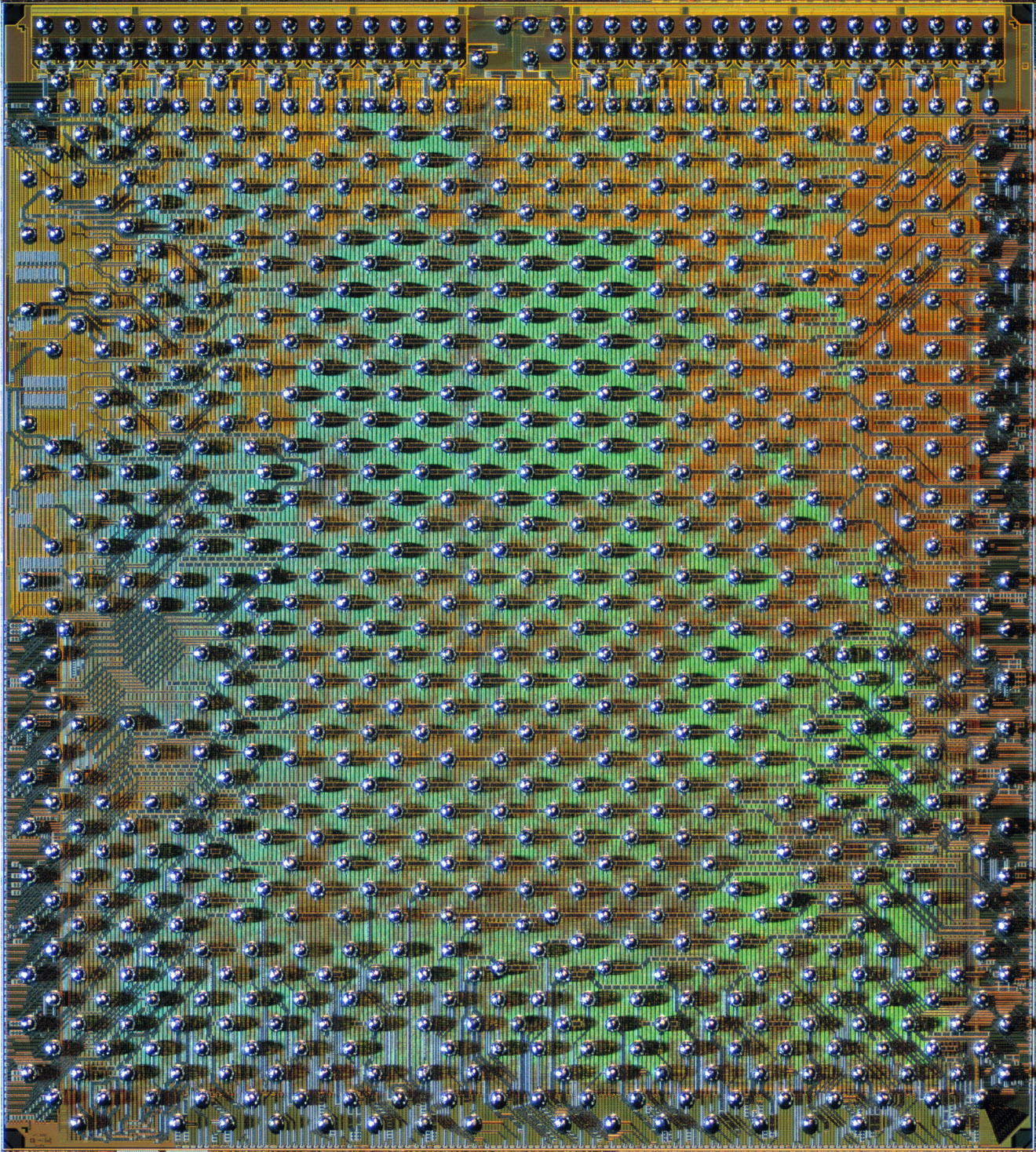
NV46 As The GeForce 6600, 2004
GeForce 6600.
In the above shot, you can actually see the bumps beneath the NV46. These bumps connect the GPU to its packaging subtrate.
* 512MB of memory
* 300 MHz Core Clock
* 500 MHz Memory Clock
* 256-bit memory bus width
-
razor512 I had a geforce fx 5900xt a long time ago, then the fan dies and since it had a lifetime warranty, I sent it in for replacement and BFG sent me back a geforce 7300GT instead (card now does a great job displaying the windows desktop on my data server)Reply -
pcxt21 Yep I'm still kicking 2 8800GTX's in SLI. Have the pants OC'd out of them now though...Reply -
tuannguyen rambo117lol, I like how the GeForce 5 series was skippedReply
No, it's because Nvidia couldn't dig up photos of it for us. -
nforce4max Hey you left out the dustbuster and a few others but ok posting.Reply
How about the NV1.
http://commons.wikimedia.org/wiki/File:NV1_GPU.jpg -
Parsian Aww i saw my old beloved GeForce MX440 64mb and GeForce TI 4600 series :PReply
never was a fan of 5000 series. ATi had much better card. I bought the ATi 9800 XT over the GeForce 5000 -
rambo117 tuannguyenNo, it's because Nvidia couldn't dig up photos of it for us.or they were too embarrassed...Reply
