Early Verdict
If you're coming from Intel's HD Graphics 530, any discrete graphics card is going to be exciting. Indeed, Radeon RX 550 looks like a great upgrade for folks limping along with CPU-based graphics. But AMD's own Radeon RX 460 2GB is quite a bit quicker than the RX 550 in demanding games, and it only costs about $10 more. If you can live with the 460's slight price premium and higher power consumption, that's the card we'd buy for $90.
Pros
- +
Low power, low heat
- +
Compact form factor
- +
Serviceable 1080p performance
- +
No auxiliary power connector
Cons
- -
Notably slower than slightly more expensive Radeon RX 460
Why you can trust Tom's Hardware Our expert reviewers spend hours testing and comparing products and services so you can choose the best for you. Find out more about how we test.
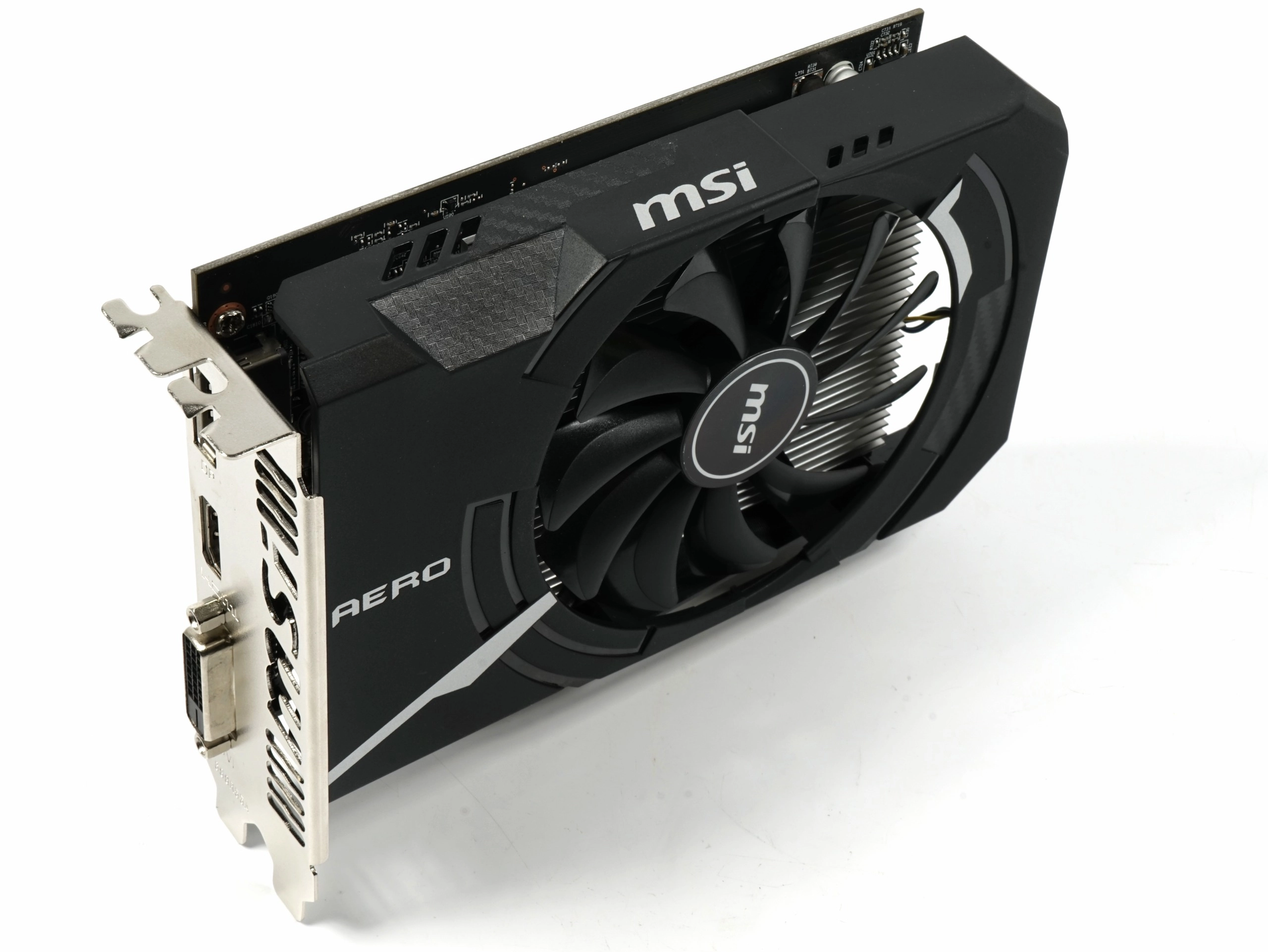
AMD Radeon RX 550 2GB
Radeon RX 550 is AMD’s first graphics card based on new silicon since its Polaris 11-based Radeon RX 460. The company says RX 550 is 1080p-capable in a number of popular e-sports games, adding that the product’s compact dimensions and low power also endear it to home-theater PCs.

Fittingly, the RX 550 slides in behind AMD’s just-announced Radeon RX 560 and starts at $80. That’s an incredibly important price point. In fact, as recently as last year, our Best Graphics recommendations included the $90 Radeon R7 360. Its disappearance forced us up the stack to Radeon RX 460, which started life at $110 last August.
Can Radeon RX 550 carve out a spot on the list of Tom’s Hardware-approved upgrades by serving up viable performance for less money than some of our past picks?
Meet Polaris 12
AMD’s older Radeon RX 460 wields 896 Stream processors. The just-announced Radeon RX 560 bumps that to 1024 Stream processors operating at even higher clock rates. When it arrives next month, we expect the RX 560 to be even faster than its predecessor for right around $100.
This leaves room for a lower-end part like the Radeon RX 550. AMD certainly could have built it using Polaris 11 with more disabled compute units. But the company’s mobile aspirations apparently necessitated a smaller GPU with fewer transistors and a more conservative power profile.
Polaris 12, code-named Lexa and based on a fourth-gen GCN architecture, is that processor. Composed of 2.2 billion transistors and measuring 101 square millimeters, it’s frankly not much smaller than Polaris 11. However, AMD plans to use it in configurations that wouldn’t have made sense from a larger chip.

In its entirety, Polaris 12 exposes 10 Compute Units organized into two Shader Engines capable of two triangles/clock, similar to Polaris 11 but with fewer CUs per Shader Engine. Radeon RX 550, specifically, uses an implementation with eight of those 10 Compute Units enabled, adding up to 512 Stream processors and 32 texture units.
The chip’s back-end is proportioned more generously, maintaining Polaris 11’s 16 ROPs, aggregate 128-bit memory bus, and 7 Gb/s GDDR5 able to move up to 112 GB/s. Whereas Polaris 11 comes with 1MB of L2 cache, however, Polaris 12 is down to 512KB.
| Header Cell - Column 0 | Radeon RX 550 | Radeon R7 260X | Radeon RX 460 |
|---|---|---|---|
| Shader Units | 512 | 896 | 896 |
| ROPs | 16 | 16 | 16 |
| GPU | Polaris 12 | Bonaire | Polaris 11 |
| Transistors | 2.2 Billion | 2.08 Billion | 3 Billion |
| Memory Size | 2GB | 2GB | 2/4GB |
| Interface | 128-bit | 128-bit | 128-bit |
| GPU Clock Rate (MHz) | 1100+ | 1100 | 1090 |
| Memory Clock Rate (MHz) | 1750 | 1625 | 1750 |
AMD’s official specification for Radeon RX 550 calls for a 1100 MHz base clock rate and 1183 MHz boost frequency, though some partners will undoubtedly configure their boards differently. A 50W ceiling exempts the RX 550 from needing an auxiliary power connector, and even at overclocked frequencies you shouldn’t have any issue staying under the motherboard slot’s specified current limit.
We are told that AMD has no plans to put any other configuration of Polaris 12 on a desktop graphics card, allowing the company to pursue mobile market share with other variants of this GPU.
Particularly relevant to Polaris 12 are some of the media and connectivity features specific to AMD's fourth-gen GCN GPUs. For more information on the architecture's display control and fixed-function accelerators, check out this page of our Radeon RX 480 8GB review.

The die markings made us do a double-take. "Made in Taiwan" doesn't indicate that Polaris 12 came from GlobalFoundries, after all. Further, the codes and font also seemed familiar from Nvidia's various processors. But it turns out that this is due to the packaging step, where the die is installed onto the GPU package. A company called ASE, which is one of the world's largest IC assemblers, handles the process, and it has offices in Taiwan. Mystery solved.
MORE: Best Graphics Cards
MORE: Desktop GPU Performance Hierarchy Table
MORE: All Graphics Content
